Among the various types of transistors, the Junction Field Effect Transistors in short JFETs holds a distinctive place due to its unique operational characteristics and versatile applications.
What is a JFET?
A Junction Field Effect Transistor (JFET) is a type of field-effect transistor (FET) that utilizes an electric field to control the flow of current. Unlike Bipolar Junction Transistors (BJTs), which are controlled by current, JFETs are voltage-controlled devices. This characteristic endows JFETs with high input impedance and low noise, making them ideal for specific applications such as amplifiers and signal processors.
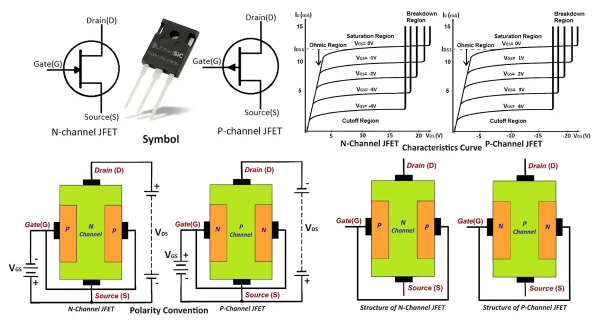
Symbol of JFET:
The circuit symbol of N-channel JFET and P-channel JFET.
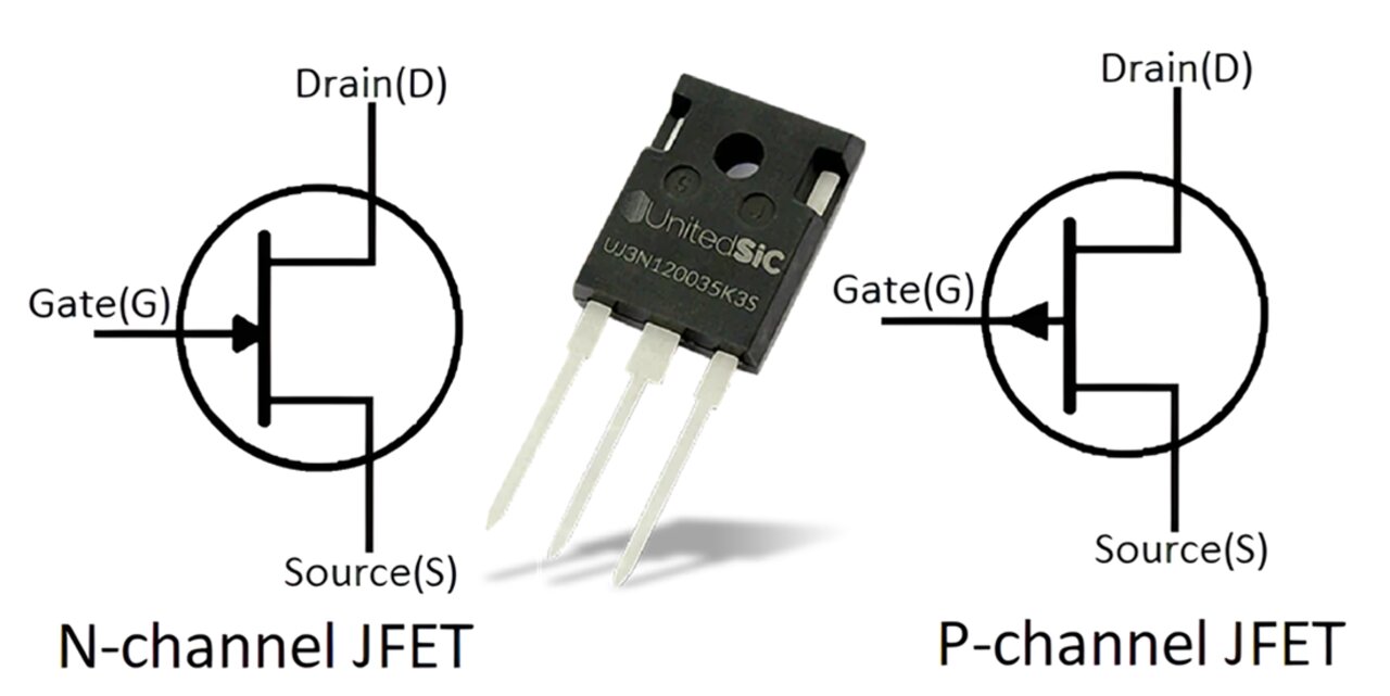
- N-channel JFET features an arrow pointing towards the gate, indicating the direction of conventional current flow when the gate is forward biased.
- P-channel JFET features an arrow pointing outwards from the gate, indicating the direction of conventional current flow when the gate is forward biased.
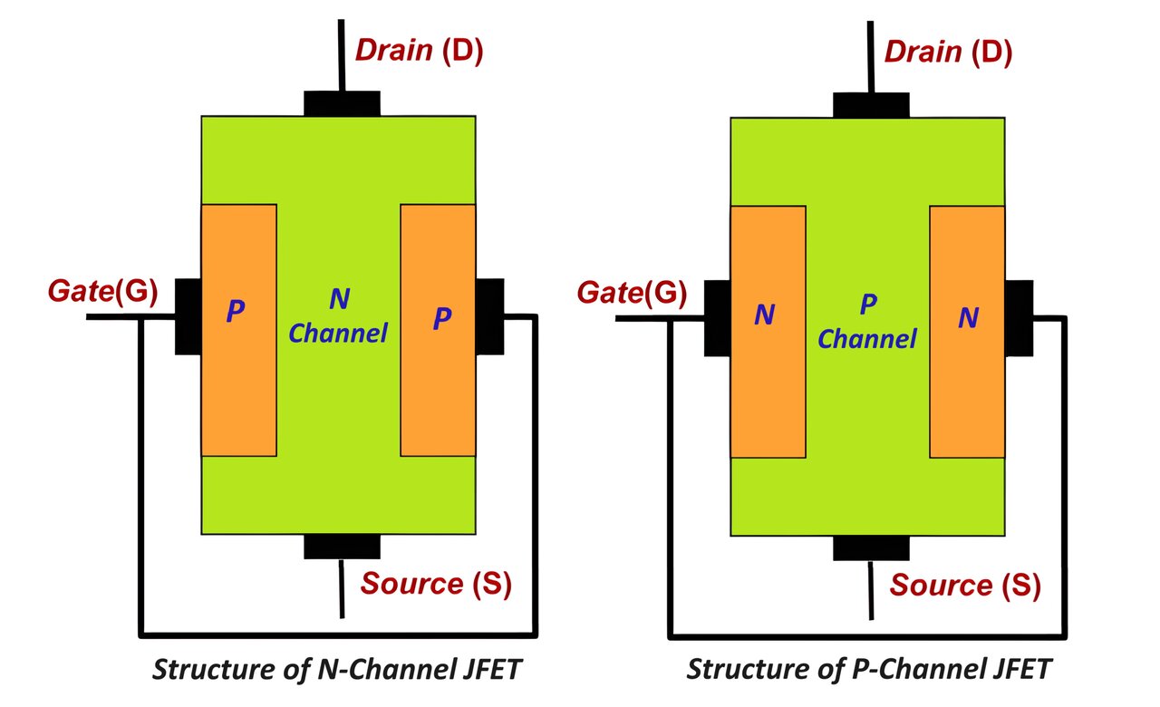
Basic Structure and Terminals of JFET:
A JFET is composed of three primary terminals and four functional regions.
Source (S): The terminal through which the majority carriers enter the channel. For N-channel JFETs, these are electrons, while for P-channel JFETs, these are holes.
Drain (D): The terminal through which the majority carriers exit the channel. The conventional current flowing out is denoted as I_D.
Gate (G): Formed by the internally connected diffused regions, it controls the flow of carriers through the channel by varying the width of the depletion regions.
Channel: The region between the source and drain through which the majority carriers flow. Its conductivity is controlled by the voltage applied to the gate.
- High Impedance: JFETs have a high input impedance, suitable for applications like amplifiers.
- Biasing: Applying an external signal to the gate terminal to set the operating point.
Types of Junction Field Effect Transistor JFET:
Junction Field Effect Transistors (JFETs) come in two primary types: N-Channel JFETs and P-Channel JFETs. These types are distinguished by the type of charge carriers that flow through their channels and the corresponding voltage polarities required for their operation. Each type has its own unique characteristics and applications.
N-Channel JFET
The N-channel JFET controls current flow through electrons.
- The N-channel JFET is primarily composed of N-type semiconductor material, forming the main body of the device.
- Source (S) and Drain (D) Terminals: These are located at opposite ends of the N-type material. The source is where the majority carriers (electrons) enter, and the drain is where they exit.
- Gate (G) Terminal: There are two small P-type regions embedded within the N-type material, which are internally connected to form the gate terminal. This creates two PN junctions within the device.
Features:
- High Electron Mobility: Due to the high mobility of electrons, N-channel JFETs typically exhibit better conductivity and faster switching times compared to their P-channel counterparts.
- Higher Conductance: They generally offer higher conductance and can handle larger currents.
P-Channel JFET
P-channel JFET relies on the movement of holes.
- The P-channel JFET is composed of P-type semiconductor material, forming the main body of the device.
- Source (S) and Drain (D) Terminals: These are located at opposite ends of the P-type material. The source is where the majority carriers (holes) enter, and the drain is where they exit.
- Gate (G) Terminal: There are two small N-type regions embedded within the P-type material, which are internally connected to form the gate terminal. This creates two PN junctions within the device.
Features:
- Hole Mobility: Holes, being the charge carriers, have lower mobility compared to electrons, which typically results in slower switching times and lower conductance for P-channel JFETs.
- Lower Conductance: They generally offer lower conductance and handle smaller currents compared to N-channel JFETs.
Construction of JFET:
A JFET consists of a thin bar of semiconductor material, which can be silicon or gallium arsenide. Regardless of whether it is an N-channel or P-channel JFET, the construction principles are similar:
- Semiconductor Bar: A bar of semiconductor material (N-type for N-channel and P-type for P-channel) forms the core structure.
- P-N Junctions: Two small regions of the opposite type (P-type for N-channel and N-type for P-channel) are diffused into the bar to create PN junctions.
- Gate Terminal: The two diffused regions are internally connected to form the gate terminal, creating a single control point for the device.
- Ohmic Contacts: The ends of the semiconductor bar form ohmic contacts with the source and drain terminals, ensuring efficient current flow.
Both N-channel and P-channel JFETs are essential in various electronic applications due to their high input impedance and ability to control current flow with minimal power consumption. Understanding their construction, operation, and characteristics is crucial for selecting the right type of JFET for specific applications, ensuring optimal performance and efficiency in electronic circuits.
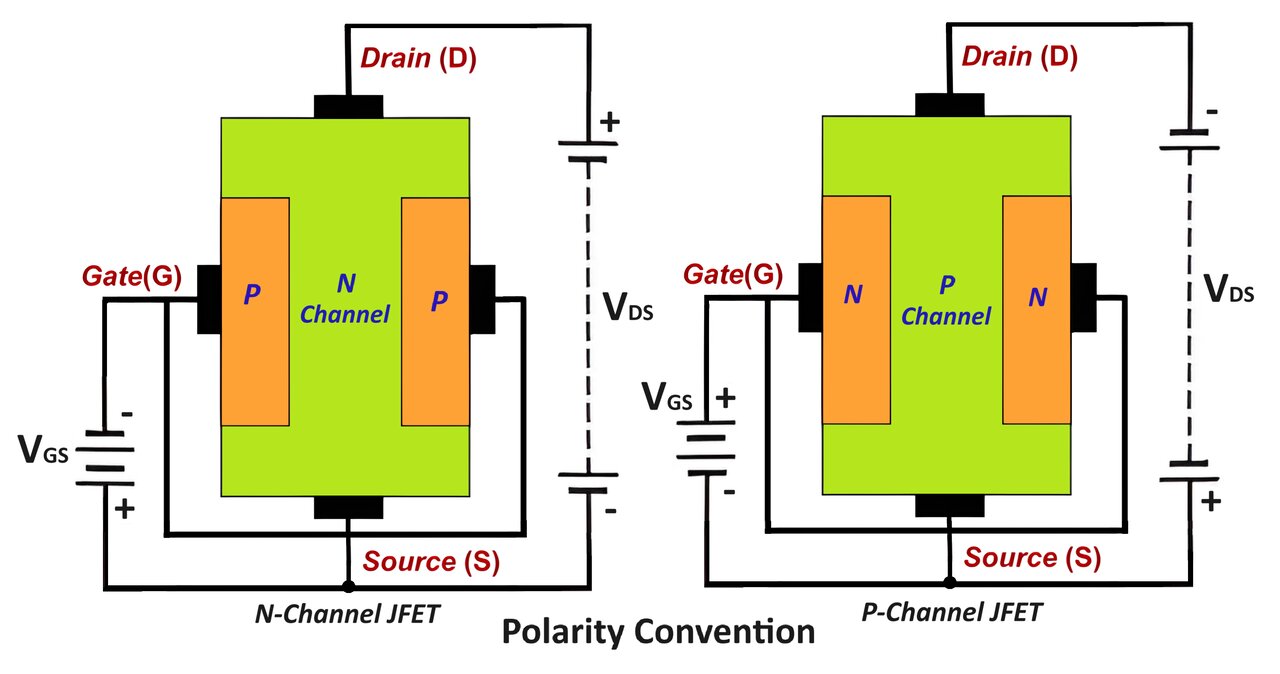
Working Principle of JFET:
JFETs operate by controlling the current flow through a semiconductor channel using an electric field. When no voltage is applied to the gate (V_GS = 0), electrons or holes can flow freely from the source to the drain. Applying a reverse voltage to the gate (negative for N-channel, positive for P-channel) creates a depletion region, narrowing the channel and increasing its resistance. By this process the flow of electrons through channel gets blocked.
Working of N Channel JFET:
- No Gate Voltage (V_GS = 0): Without any gate-source voltage, the channel is open, and electrons flow freely from the source to the drain, allowing maximum current (I_D) through the device.
- Negative Gate Voltage (V_GS < 0): Applying a negative voltage to the gate relative to the source widens the depletion regions of the PN junctions, narrowing the channel and increasing its resistance. This reduces the drain current (I_D). As V_GS becomes more negative, the channel constricts further until it is completely “pinched off,” stopping current flow.
Working of P Channel JFET:
- No Gate Voltage (V_GS = 0): Without any gate-source voltage, the channel is open, and holes flow freely from the source to the drain, allowing maximum current (I_D) through the device.
- Positive Gate Voltage (V_GS > 0): Applying a positive voltage to the gate relative to the source widens the depletion regions of the PN junctions, narrowing the channel and increasing its resistance. This reduces the drain current (I_D). As V_GS becomes more positive, the channel constricts further until it is completely “pinched off,” stopping current flow.
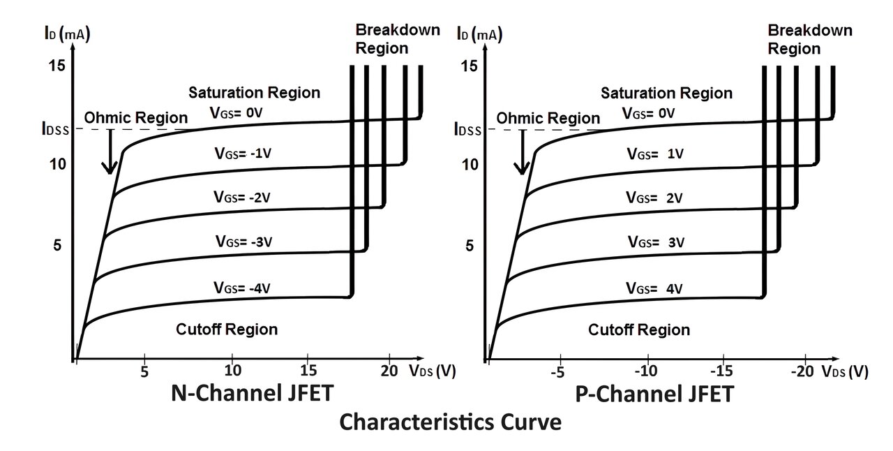
VI Characteristics of JFET:
Output Characteristics:
- Saturation Region: Low V_DS; the current is constant and controlled by V_GS.
- Ohmic Region: V_DS increases, and current increases linearly.
- Pinch-Off Region: The channel narrows, and current becomes independent of V_DS.
- Breakdown Region: Excessively high V_DS causes uncontrolled current flow.
- V_GS = 0: The channel is fully open, allowing maximum current flow (I_D).
- Negative V_GS (for N-channel): Increases the depletion region, reducing channel width and current flow.
- Positive V_GS (for P-channel): Similar effect, increasing the depletion region and reducing current flow.
- Pinch-off Voltage: The gate voltage at which the channel is completely closed, and current flow stops.
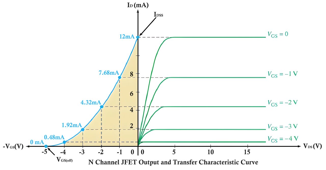
Transfer Characteristics:
- Plot between I_D and V_GS, keeping V_DS constant.
- Shows how drain current (I_D) varies with gate-source voltage (V_GS).
- Negative Slope (N-channel JFET): In N-channel JFETs, as the gate-source voltage (VGS) becomes more negative, the drain current (ID) decreases. This negative relationship is characteristic of N-channel JFETs.
- Positive Slope (P-channel JFET): Conversely, in P-channel JFETs, the drain current (ID) increases as the gate-source voltage (VGS) becomes more negative. This positive relationship is typical of P-channel JFETs.
Advantages and Disadvantages of JFET:
Advantages of Junction Field Effect Transistors JFET:
High Input Impedance: JFETs don’t put much load on previous circuits, making them great for amplifiers.
Low Noise: They produce less electrical noise, perfect for sensitive signal processing like in audio devices.
Low Power Consumption: They use very little power, making them energy-efficient and suitable for battery-powered devices.
Simplicity: They’re easier to use in circuits compared to other transistors, reducing complexity and cost.
No Gate Current: JFET gates don’t need much current, simplifying circuit designs.
Temperature Stability: They remain stable over different temperatures, ensuring reliable performance.
Disadvantages of Junction Field Effect Transistors JFETs:
Limited Gain: They don’t amplify signals as much as other transistors, limiting their use in high-amplification circuits.
Gate-Source Leakage: They can have small leakage currents, which might be a problem in circuits requiring very low currents.
Limited Frequency Response: They might not work well at very high frequencies compared to other transistors.
Lower Conductance: Especially in P-channel JFETs, they may not handle large currents as well due to lower conductance.
Unipolar Device: They only rely on one type of charge carrier, limiting their versatility compared to other transistors.
Cost: They can be more expensive than other transistors, affecting the overall cost of electronic designs.
Applications of Junction Field Effect Transistors JFET:
1. Amplifiers
- Low-Noise Amplifiers: JFETs are used in applications where minimizing electrical noise is crucial, such as in audio equipment, microphones, and communication devices.
- High-Impedance Preamplifiers: Due to their high input impedance, JFETs are ideal for preamplifiers that need to interface with high-impedance sensors like piezoelectric sensors and certain types of microphones.
2. Switching Circuits
- Electronic Switches: JFETs function effectively as switches in low-power and high-frequency applications. They can turn on and off rapidly, making them suitable for use in RF switching circuits and other digital applications.
- Analog Switches: JFETs can be used in analog switching applications, where they control the routing of analog signals with minimal distortion.
3. Sample and Hold Circuits
- Signal Sampling: JFETs are used in sample-and-hold circuits to sample the input signal and maintain (or hold) its value for a period of time, crucial in analog-to-digital conversion processes.
4. Voltage Regulators
- Stable Voltage Supply: JFETs help in maintaining a stable output voltage despite variations in input voltage or load conditions. This is essential in power supply circuits where consistent voltage is necessary for reliable operation of electronic devices.
5. Oscillators
- Waveform Generation: JFETs are key components in oscillator circuits used to generate repeating waveforms, such as sine waves, square waves, and other periodic signals. They are used in applications like signal generators and clock circuits.
- Frequency Control: JFETs can be used to control the frequency of oscillators, ensuring stable and precise frequency generation.
6. Buffer Circuits
- Impedance Matching: JFETs are used in buffer circuits to provide impedance matching between different stages of a circuit, ensuring signal integrity and preventing signal loss.
7. Voltage-Controlled Resistors
- Variable Resistance: JFETs can function as voltage-controlled resistors, where the resistance between the drain and source can be varied by adjusting the gate voltage. This is useful in applications like automatic gain control circuits.
8. Current Limiters
- Current Control: JFETs can be used in circuits to limit the current, protecting sensitive components from excessive current that could cause damage.
JFET Summary:
The Junction Field Effect Transistor (JFET) is a fundamental component in electronics, operating on the principle of electric field control.
It is a three-terminal device consisting of the gate, drain, and source terminals.
The gate serves as the control terminal, regulating the flow of current between the drain and source.
JFETs are used in amplifier circuits, switching circuits, signal processors and controlling power in various electronic devices.
There are two types of JFETs: N-channel JFET and P-channel JFET. The N-channel JFET controls current flow through electrons, while the P-channel JFET relies on the movement of holes.
Selecting the appropriate type of transistor involves considering factors like voltage, current, frequency, and impedance to achieve optimal performance.
JFETs have high input impedance, low noise, and efficient power consumption. Understanding their characteristics, working principles, and applications is crucial for engineers and enthusiasts to innovate and advance technology.
IGBT Full Form, Symbol, Construction, Working and Applications
