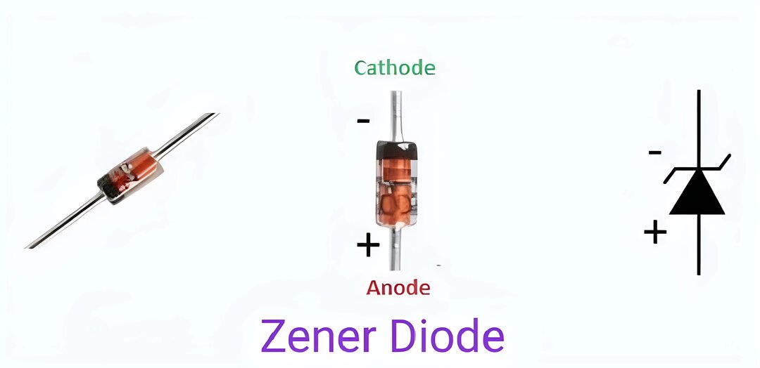
Here we will discuss the VI characteristics of Zener Diode, its working as a voltage regulator and some applications. Zener Diode is a special purpose PN junction diode its construction is similar to a conventional PN junction diode. It has some unique characteristics which we will discuss.
Overview of Zener Diode as Voltage Regulator:
Zener diode is a special type of Diode specifically designed to operate in reverse biased mode. Zener diodes are available in the range from 3V to 200 Volts. They are operated in a breakdown region hence they are called breakdown diode.
The reverse breakdown voltage of the Zener diode adjusts by doping level.
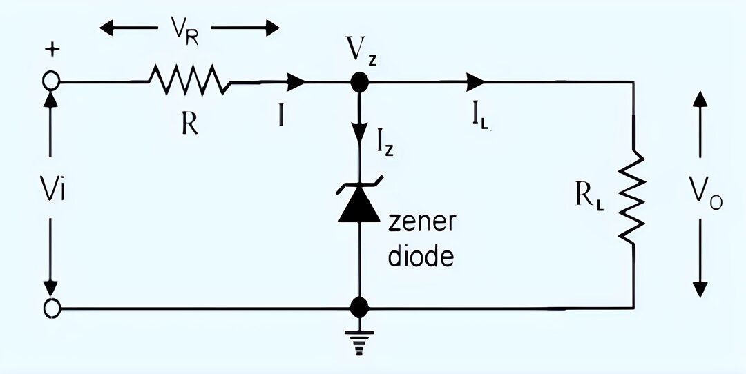
Zener diode in voltage regulator Circuit:
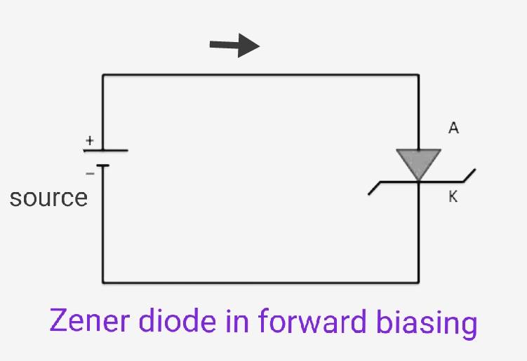
Biasing of Zener Diode:
Biasing of Zener diode is as shown in the figure.
a.) In forward bias mode it behaves like a normal Diode but normally it is not used in forward direction.
Symbol of Zener Diode in forward bias mode:
b.) When Zener diode is reverse biased it Behaves as a Voltage regulator. when Voltage across Zener diode is increased above its reverse breakdown voltage it starts conducting and reduces Voltage across it by acting short-circuited.
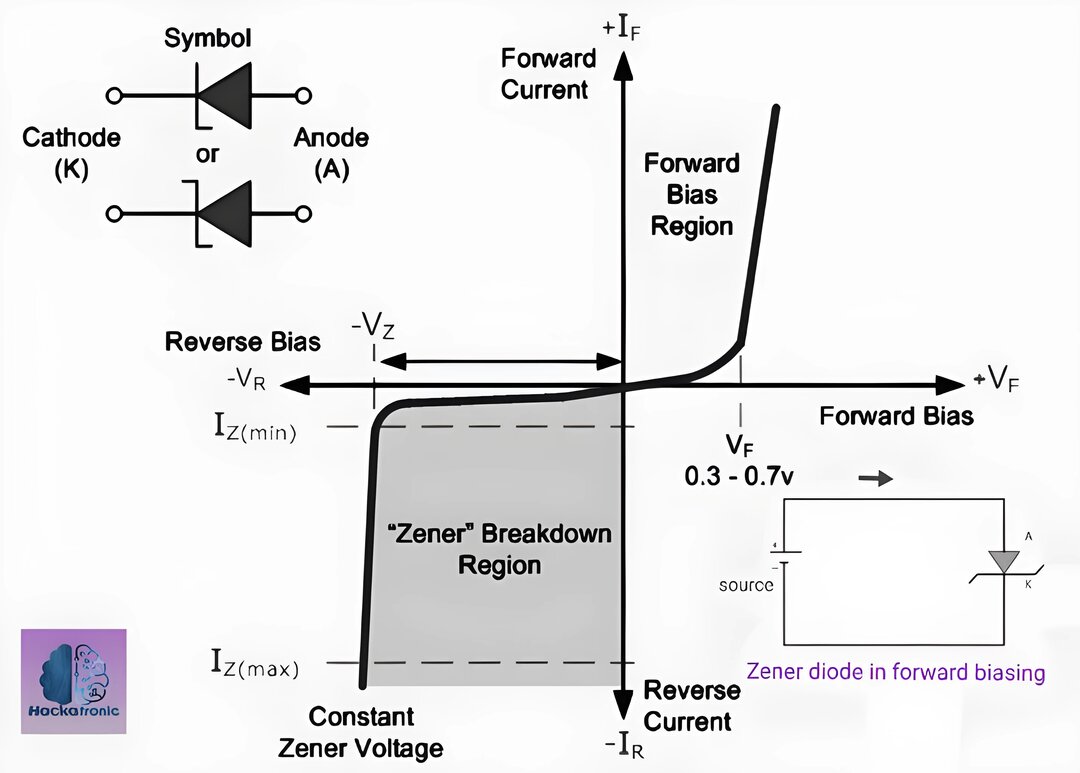
VI Characteristics of Zener Diode:
1.) Forward characteristics of Zener diode
Forward characteristics of PN junction diode is similar to a conventional PN junction diode.
2.) Reverse characteristics of Zener diode
The reverse characteristics of Zener diode are entirely different from normal PN junction diode. As shown in the graph
If we increase the reverse voltage initially a small current in micro-ampers flows. This current flows due to thermally generated minority carriers.
At a certain value of reverse Voltage, current will increase suddenly and sharply. This indicates that breakdown has occurred this breakdown voltage is known as Zener breakdown voltage Vz. This reverse breakdown voltage can be controlled precisely by adjusting the doping level at the time of manufacturing.
After the breakdown has occurred voltage across the Zener diode remains constant equal to Vz. Any increase in Zener Voltage will result in an increase in reverse Zener current.
After reverse breakdown current must be controlled by connecting a resistor in series with the Zener diode this is very important to avoid damage to the diode due to heating.
The load is always connected in parallel with the Zener diode so that the voltage across the load is equal to Zener voltage Vz.
The supply voltage Vs is always greater than the Zener voltage Vz.
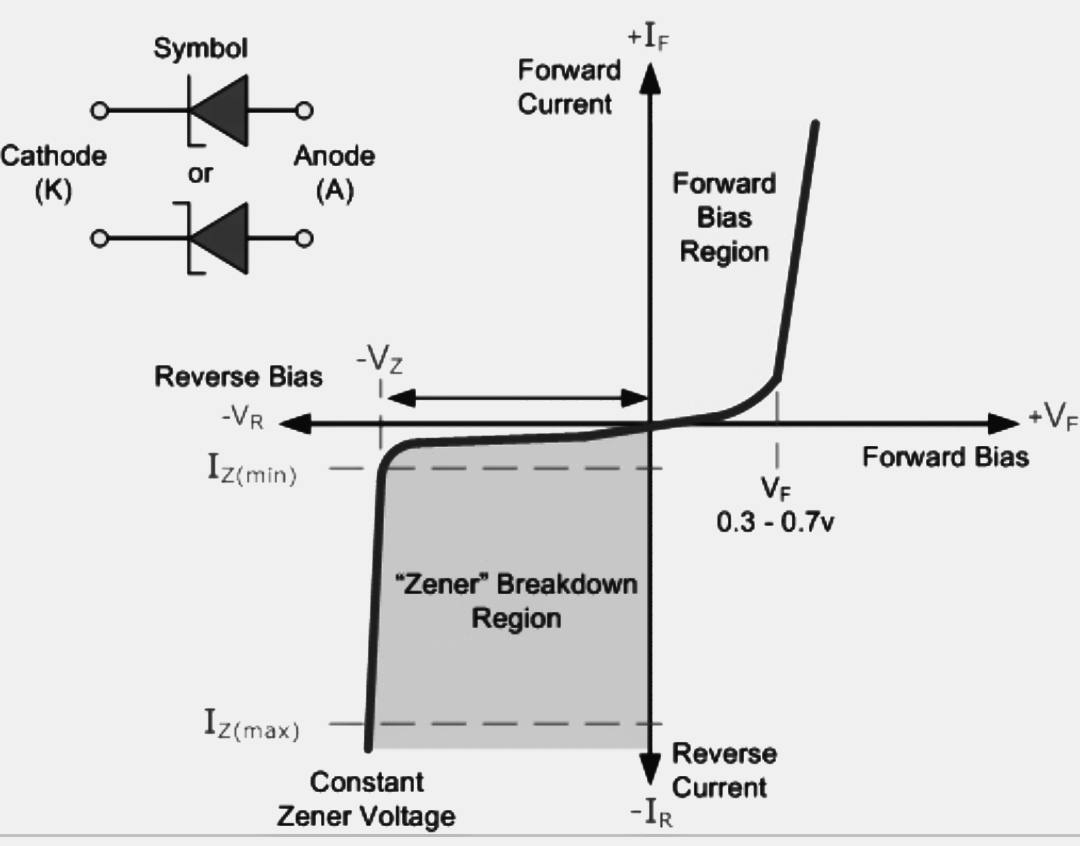
Importance of Zener breakdown region
After breakdown Zener diode operates in the breakdown region. In the breakdown region, Zener diode works as a Voltage regulator by adjusting current flowing through it when Voltage across it becomes greater than breakdown voltage Vz.
As shown in the graph
To understand the working of Zener diode let’s first understand
what is Zener breakdown? And what is the avalanche breakdown?
Avalanche Breakdown and Zener Breakdown
Zener breakdown:
Zener breakdown is observed in Zener diode having vz less than 5-volt aur between 5 to 8 volts let’s understand the Zener breakdown mechanism for Vz less than 5 volts.
A very intense electric field appears across the narrow depletion region when a voltage of 5 volts or less is applied to the zener diode.
This intense electric field is strong enough to pull some of the valence electrons into the conduction band by breaking their covalent bonds, electrons then become free which are available for conduction.
A large number of such free electrons will constitute large reverse current through the zener diode. breakdown is said to have occurred due to zener effect.
to avoid damage of diode due to excessive heating a resistor should be connected in series with the zener diode.
The Zener breakdown voltage also depends on the temperature of junction if the junction temperature increases then the Zener breakdown voltage decreases.
The v-i characteristic is very sharp after the breakdown has occurred.
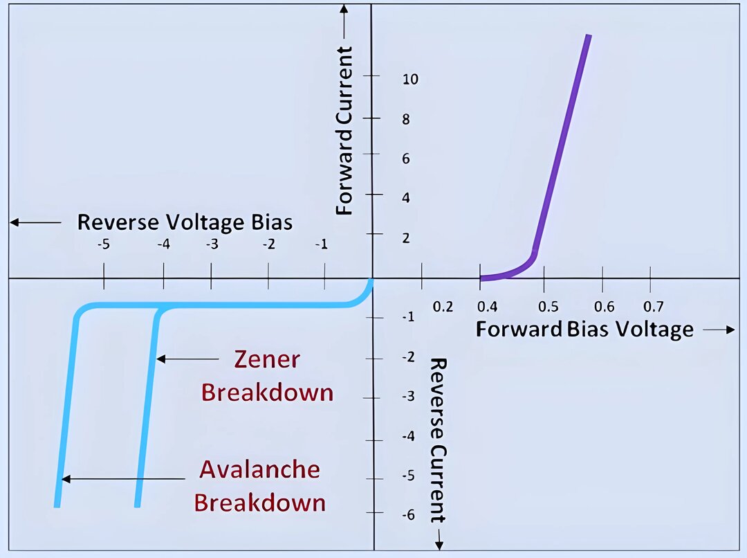
Avalanche breakdown in Zener Diode:
Avalanche breakdown is observed in zener diode when Vz is higher than 8 volts.
in the reverse biased condition, the conduction of current will take place only due to minority carriers.
As we increase the reverse voltage applied to the zener diode these minority Carriers will tend to accelerate, there for kinetic energy associated with these electrons will increase.
While traveling these accelerated minority Carriers will collide with the stationary atoms and transfer some of their kinetic energy to the valence electrons present in the covalent bonds.
Due to this additionally acquired energy the valence electrons will break their covalent bonds and jump into the conduction band to become free for conduction.
Now this newly generated free electrons will get accelerated they will knock out some more valence electron by means of collision, this phenomenon is called as carrier multiplication.
Due to carrier multiplication process a large number of free minority carrier electrons and holes will be available for the conduction and the carrier multiplication process become self-sustained continuous process.
This continuous carrier multiplication process is called as avalanche effect a large rivers current start flowing through the Zener diode. This is called avalanche breakdown. To protect diode against damage due to excessive heating a current limiting resistor should be connected in series.
The breakdown voltage in avalanche breakdown increases with increase in the junction temperature.
The v-i characteristic of reverse biased region with avalanche breakdown is shown in the graph which shows that the characteristic has a gradually increasing nature.
Application of Zener diode:
1.) As a Voltage reference in emitter follower type Voltage regulator.
2.) As a regulated power supply.
3.) In the protection circuit for MOSFET and OPAMPs.
4.) In clipping and wave shaping circuits.
5.) In pulse amplifiers.
Universal NOR Gate Truth Table, Logic Circuit and IC PIN Diagram

it was useful for me 🙂