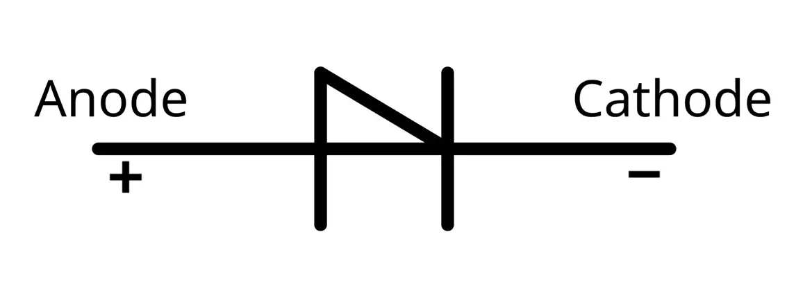
You can see Shockley diode symbol it is a four-layer (P-N-P-N) semiconductor device. Like pn junction diode It conducts in forward bias and stops conducting in reverse bias. The main difference between a conventional diode and a Shockley diode is, it starts conducting when the forward voltage crosses its breakdown voltage. It is an active component. It is named after its inventor William Bradford Shockley.
Shockley was the first semiconductor device invented which was a “pnpn” diode. (Types of Diodes and symbol) It is equivalent to a thyristor without a gate. Shockley Diode is not widely because of many alternate devices like Diac, Triac, and SCR. These devices work on the principle of the Shockley diode.
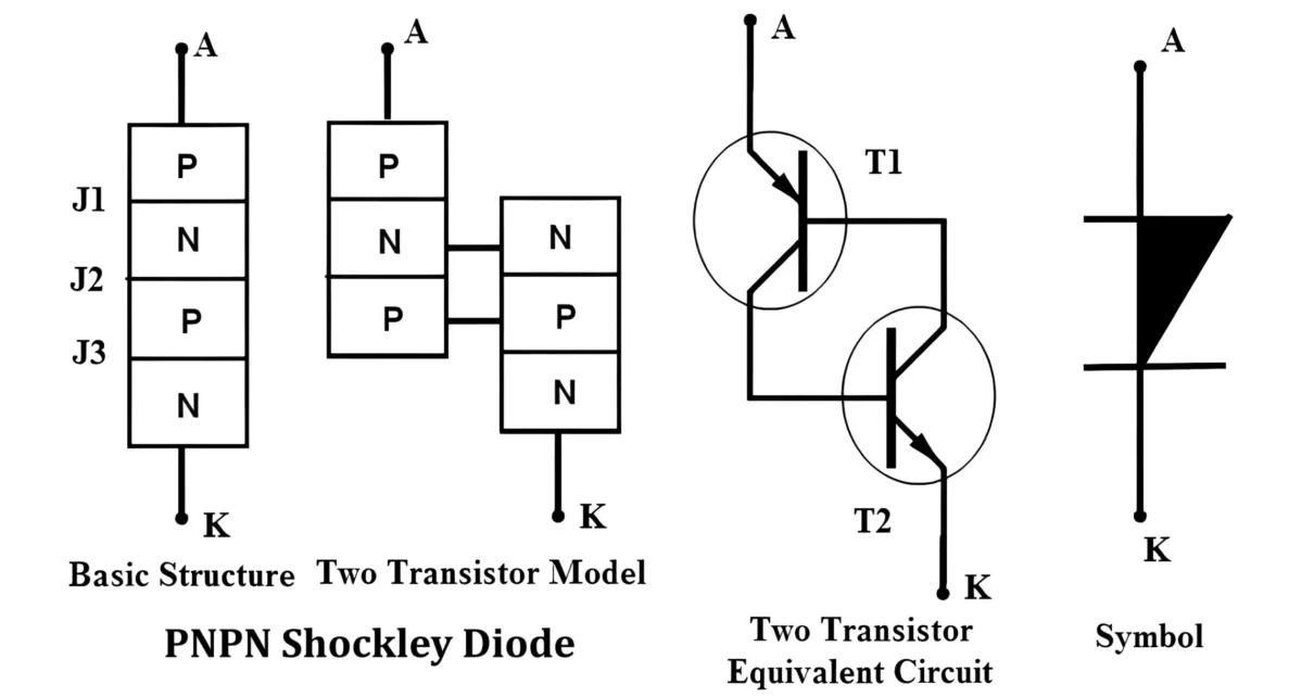
It is a two-terminal device hence it is called as diode. It is used as a switch, it operates in two states either ON or OFF. because of its construction It is also called PNPN diode. It is a two-terminal device hence it is called as diode.
Construction of Shockley Diode
It is formed by sandwiching four layers of semiconductor material. NPNP or PNPN vice versa. Three junctions are formed due to the diffusion of four layers. The internal structure and symbol of Shockley diode is as shown in the figure.
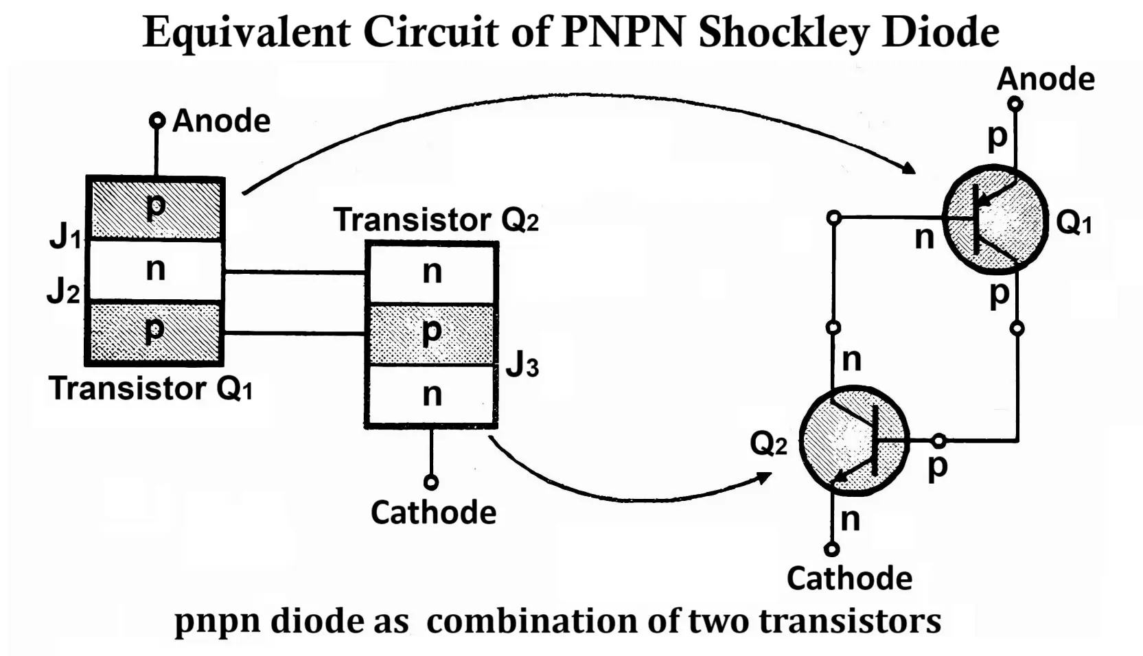
The construction of Shockley diode can also be understood by two transistor analogy.
the two-transistor equivalent circuit of a four-layer diode is as shown in the figure. the pnpn diode has been split into two parts which are separated mechanically but connected electrically. It shows that the four-layer diode can be considered as two transistors which are connected back to back. The transistor Q1 is a PNP transistor and a transistor Q2 is an NPN transistor. The collector of one transistor is connected to base of the other and vice versa.
The junction J1 is emitter-base junction, junction J2 base – collector or collector-base junction and junction j3 is base -emitter junction. Junction J2 is common to both transistors.
In forward bias mode junction J1 and J3 are forward biased and junction J2 is reverse biased. Shockley diode is operated in forward bias mode only. In reverse-biased mode junction J1 and J3 are reverse biased and junction J2 is forward-biased. In reverse biasing if reverse voltage increases above breakdown voltage the diode gets damage.
Working of Shockley Diode:
a.) Operation in forward biased:
Due to the four alternate layers, there are three junctions in the Diode. When an external voltage is applied to make the anode positive with respect to cathode, the junctions J1 and J3 are forward biased and junction J2 is reverse biased.
The externally applied voltage appears almost completely across the reverse biased junction J2. A very small current (leakage current) will flow through the diode.
As we increase the external voltage, the diode current increases slowly. This will continue upto a voltage called “firing voltage” or “breakover voltage” Vbo. When the current increases to a particular value the diode switches to ON state. This value of current is called holding current in Shockley diode.
As soon as the applied voltage becomes equal to the breakover voltage, the diode current increases sharply and the voltage across the device decreases sharply.
This happens due to breakdown of junction J2 at the breakover voltage.
Thus, at the breakover point the p-n-p-n diode switches from OFF state to ON state. This is shown in the VI characteristics.
b.) Operation when reverse biased:
When reverse biased the p-n-p-n diode acts like a typical p-n junction diode. Junction J1 and J3 are reverse biased and junction J2 is forward biased. The current flowing through the device is very small leakage current.
If the reverse voltage reaches the reverse breakdown voltage, then the device breaks down and a large current flows through it and diode gets damaged.
Resistance offered by the diode:
The four-layer diode acts basically as a switch. Therefore, it has two stable states. In reverse bias it acts like an open switch and offers a very high resistance typically of 100 MΩ. When forward-biased, it is equivalent to a closed switch and offers a resistance less than 10Ω.
V-I characteristics of Shockley diode
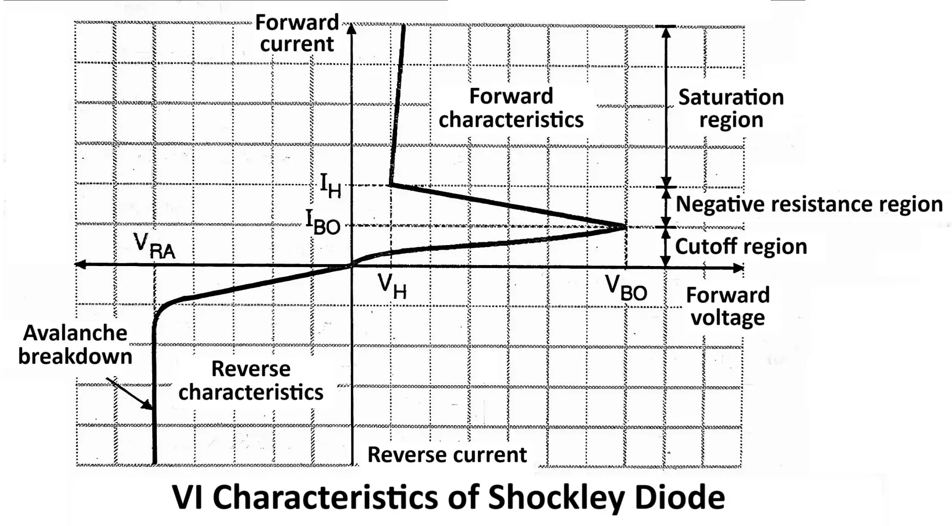
Reverse characteristics:
When the voltage is applied in the reverse direction, the junctions J1 and J3 are reverse-biased. At a high reverse voltage breakdown will occur at these junctions. This voltage is termed as reverse avalanche voltage VgA. When the reverse voltage is less than Ve. a small leakage current flows through the device due to the thermally generated minonty carrers.
This reverse current is therefore temperature dependent. The shape of the reverse characteristics is same as that of a p-n junction diode.
Forward characteristics:
The forward characteristics can be divided into two categories:
1. Cut-off region or forward blocking region.
2. Negative resistance region.
3. Saturation region.
When the four-layer diode is forward biased, a small forward current flows until the voltage reaches the breakover voltage Vbo and the corresponding current is Ibo.
As soon as forward voltage reaches Vbo the device current increases suddenly and the voltage across the device drops to a low value.
The device thus enters into the negative resistance region for a very short time. It quickly switches into the saturation region or the ON state. The ON state is a low voltage, high current, low resistance region. The voltage across the device in this state is very low.
Once the diode enters into the ON state or saturation region, it gets “latched”.
Even if the forward voltage is reduced the diode remains ON as long as the forward current is less than the “holding current” Ig. Ig is the minimum current required to hold the diode in its ON state.
How to Turn OFF?
A conducting Shockley diode can be turned off by either applying a reverse voltage (anode to cathode) across the conducting device or by reducing the forward current below the holding current value.
Advantages of Shockley Diode:
1.) Simple construction.
2.) Gets latched into the on state
3.) Low forward voltage drop hence low power dissipation.
4.) Capable of blocking the reverse voltage.
5.) It can be protected against over-current with the help of a fuse.
Disadvantages of Shockley Diode:
1. Conducts in only one direction.
2.) Can turn on accidentally due to rate effect.
3.) Not easy to turn off.
Can not switch at a fast speed.
There is no control over the forward breakdown voltage.
4.) It does not have any control terminal.
Applications of Shockley Diode:
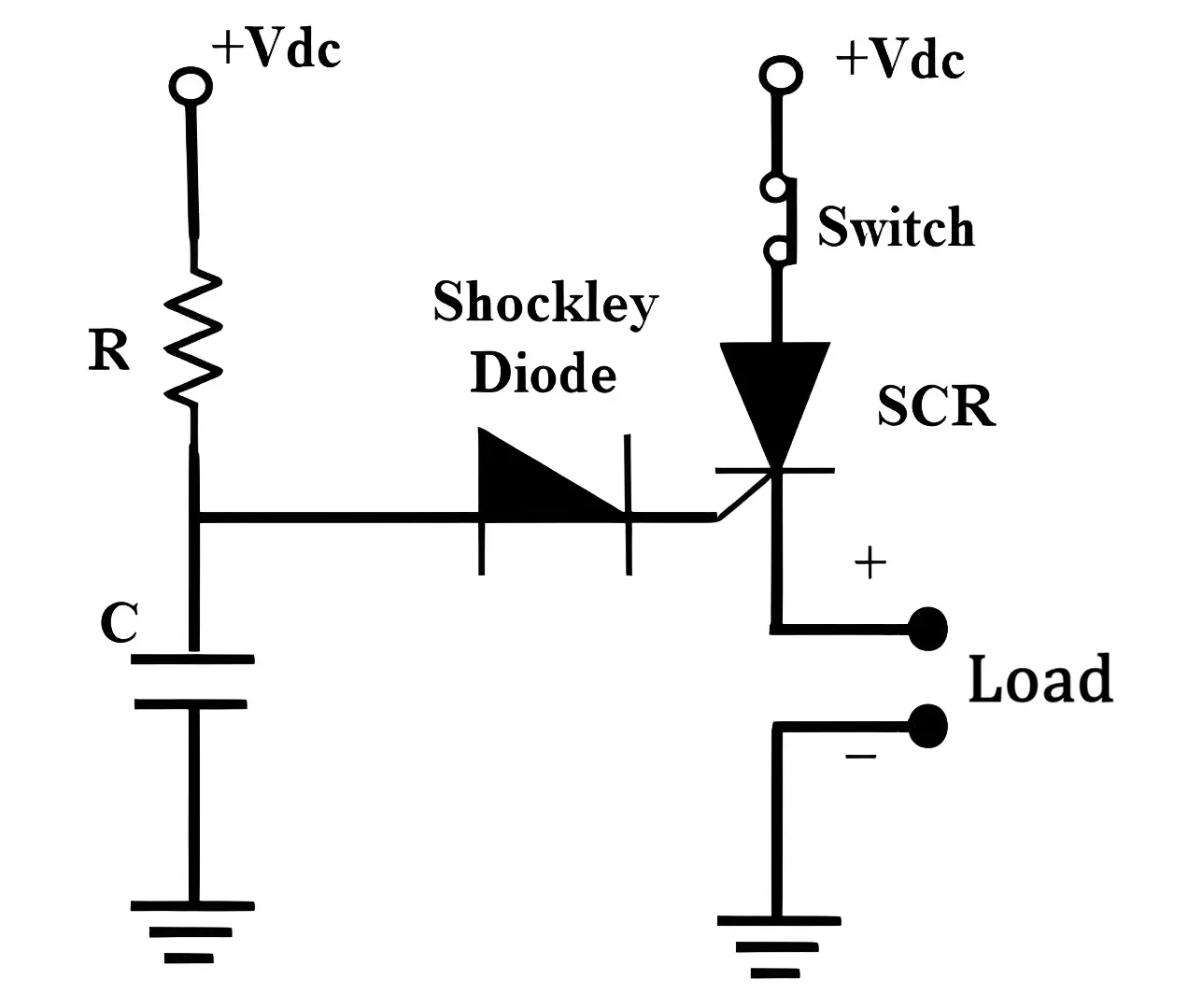
As a Trigger Switch:
The most common application of the Shockley diode is the trigger switch in which it is used to turn on the SCR.
As we turn on the circuit, the RC network is fed to DC supply and capacitor starts charging. capacitor C starts charging towards Vdc Via R.
When Vc = Vbo of the diode, it turns on to provide the gate current pulse to SCR and turns on the SCR. Once the SCR is turned on it remains in the latched state, the Shockley diode is used only to turn on SCR.
In Relaxation Oscillator:
Relaxation oscillator circuit using a Shockley diode. In this the diode is connected in parallel to capacitor power with a power supply battery.
As the voltage is applied the capacitor starts charging through a resistance R. When the voltage across the capacitor becomes more than the breakover voltage of Shockley diode, it becomes short-circuited and turns ON acting as a Switch.
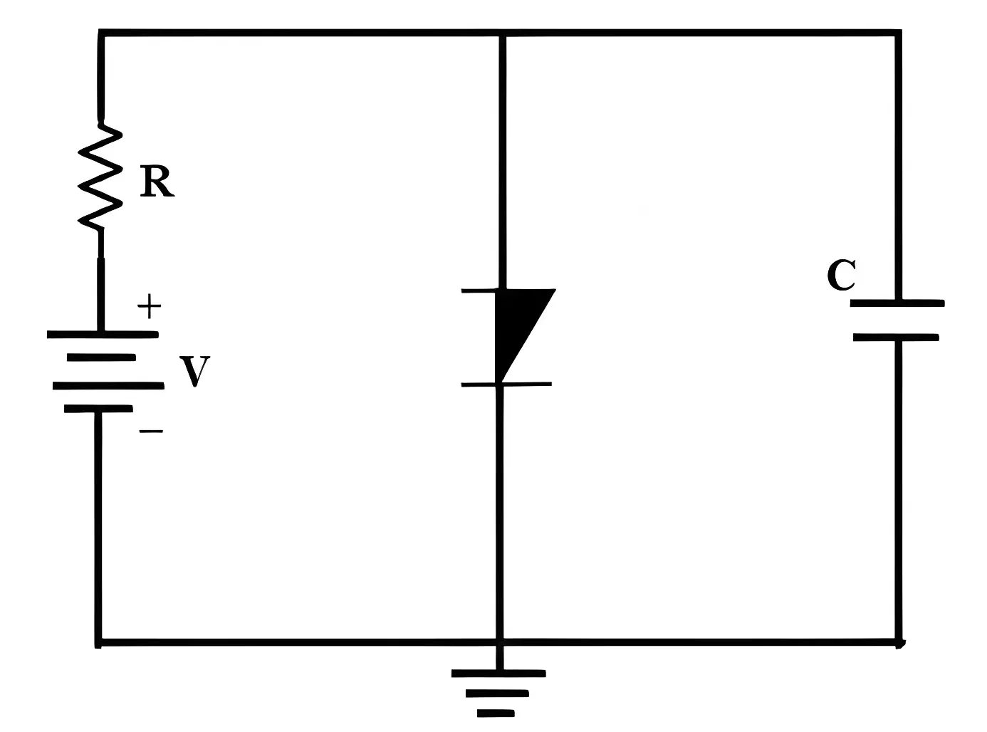
This causes rapid discharge of capacitor through the diode. As the current through the diode is less than the holding current, the diode turns OFF and capacitor starts charging again.
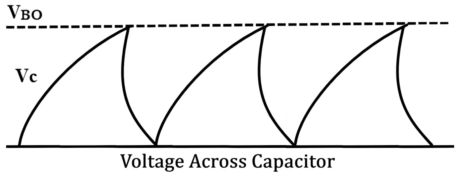
The voltage variation across the capacitor is as shown in the graph voltage across the capacitor is always greater than zero.
If any query, then feel free to ask us…
Also watch this PPT on Shockley Diode
