The MOS Capacitor (Metal Oxide Semiconductor Capacitor) is the fundamental electrostatic structure underlying modern semiconductor devices. Every MOSFET, CMOS integrated circuit, DRAM cell, Flash memory array, and nanoscale logic transistor originates from MOS capacitor physics.
Understanding MOS capacitor behavior, electrostatics, energy band behavior, and Capacitance Voltage (CV) characteristics is essential for:
- Semiconductor device physics
- VLSI circuit design
- Integrated circuit fabrication
- Process monitoring and characterization
- Threshold voltage engineering
What is a MOS Capacitor
A MOS capacitor is a voltage-controlled capacitor formed by stacking three layers:
- Metal or polysilicon gate
- Thin insulating oxide layer
- Semiconductor substrate
Unlike a conventional parallel plate capacitor where both plates are conductors, one terminal here is a semiconductor. Because charge carriers inside a semiconductor are mobile and voltage dependent, the capacitance varies with applied gate voltage.
Related Articles
- MOSFET VI Characteristics, Symbol and it’s Classification
- Difference Between D-MOSFET and E-MOSFET Explained
- Difference Between BJT and MOSFET | (BJT vs MOSFET)
- IGBT Full Form, Symbol, Construction, Working and Applications
- Bipolar Junction Transistors (BJT) Working and Applications
MOS Capacitor Structure
- Metal Gate
- Originally aluminum metal
- Modern technologies use heavily doped polysilicon or metal gates
- Acts as the control terminal
- Determines work function and flat band voltage
- Oxide Layer
- Typically Silicon Dioxide SiO₂
- Thickness ranges from a few nanometers in advanced CMOS
- Acts as dielectric
- Blocks DC current flow
- Allows electric field penetration
- Semiconductor Substrate
- Can be p type substrate for NMOS analysis
- Can be n type substrate for PMOS analysis
Cox = (εox × A) / tox
- εox = permittivity of oxide material
- A = capacitor area
- tox = oxide thickness
- Cox = oxide capacitance
MOS Capacitor as Voltage Controlled Device
- When gate voltage VG is applied:
- An electric field forms across oxide
- Surface potential changes
- Charge carriers redistribute
- Effective capacitance changes
- MOS capacitance is voltage dependent.
Electrostatics and Poisson Equation
The electrostatic behavior of the MOS capacitor is governed by Poisson equation inside the semiconductor:
d2ψ(x)/dx2 = −ρ(x) / εs
- ψ(x) = electrostatic potential
- ρ(x) = charge density
- εs = semiconductor permittivity
Under depletion approximation, charge density is assumed constant and equal to ionized dopant concentration.
Depletion Width Derivation
Wd = √((2εsψs) / (qNA))
- Wd = depletion width
- ψs = surface potential
- q = electron charge
- NA = acceptor concentration
This shows depletion width increases with surface potential and decreases with heavier doping.
Operating Regions of MOS Capacitor
An n-channel enhancement-mode MOSFET fabricated on a p-type substrate operates through three fundamental bias regions: accumulation, depletion, and inversion, where the surface carrier distribution and gate-to-substrate capacitance vary as a function of the applied gate voltage.
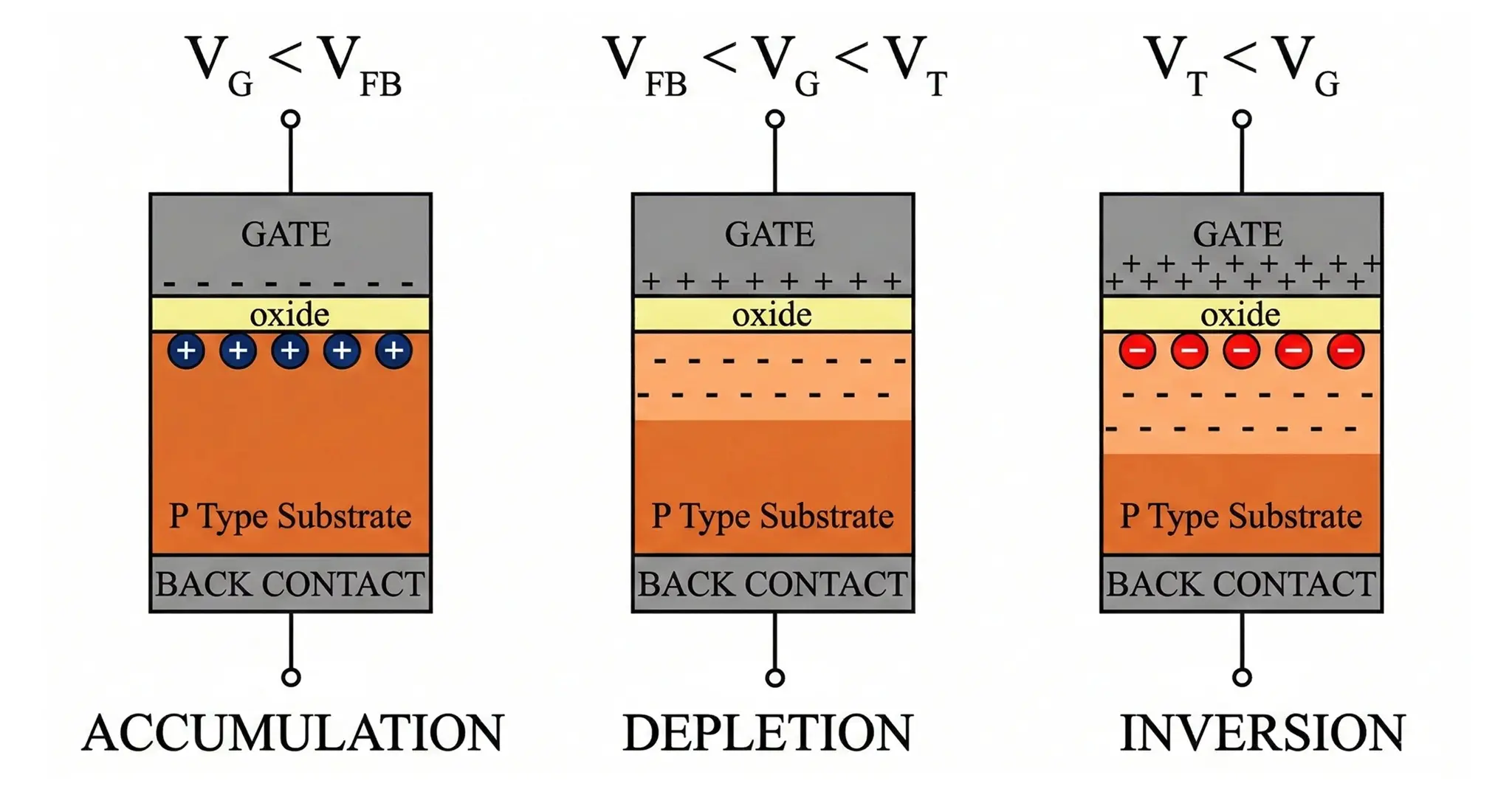
- Negative gate voltage VG → Accumulation
- Small positive gate voltage VG → Depletion
- Large positive gate voltage VG → Inversion
Accumulation Region
VG < VFB
Negative gate voltage attracts holes to the oxide semiconductor interface.
- Majority carriers accumulate
- No depletion region forms
- Semiconductor behaves like conductor
CMOS ≈ Cox
Depletion Region
VG > VFB
Positive gate voltage repels holes from surface.
- Mobile carriers removed
- Fixed ionized acceptor ions remain
- Depletion width increases with voltage
CMOS = (Cox × Cd) / (Cox + Cd)
- Cd = depletion capacitance
- CMOS = total measured capacitance
Depletion capacitance:
Cd = εs / Wd
Inversion Region
VG ≥ VTH
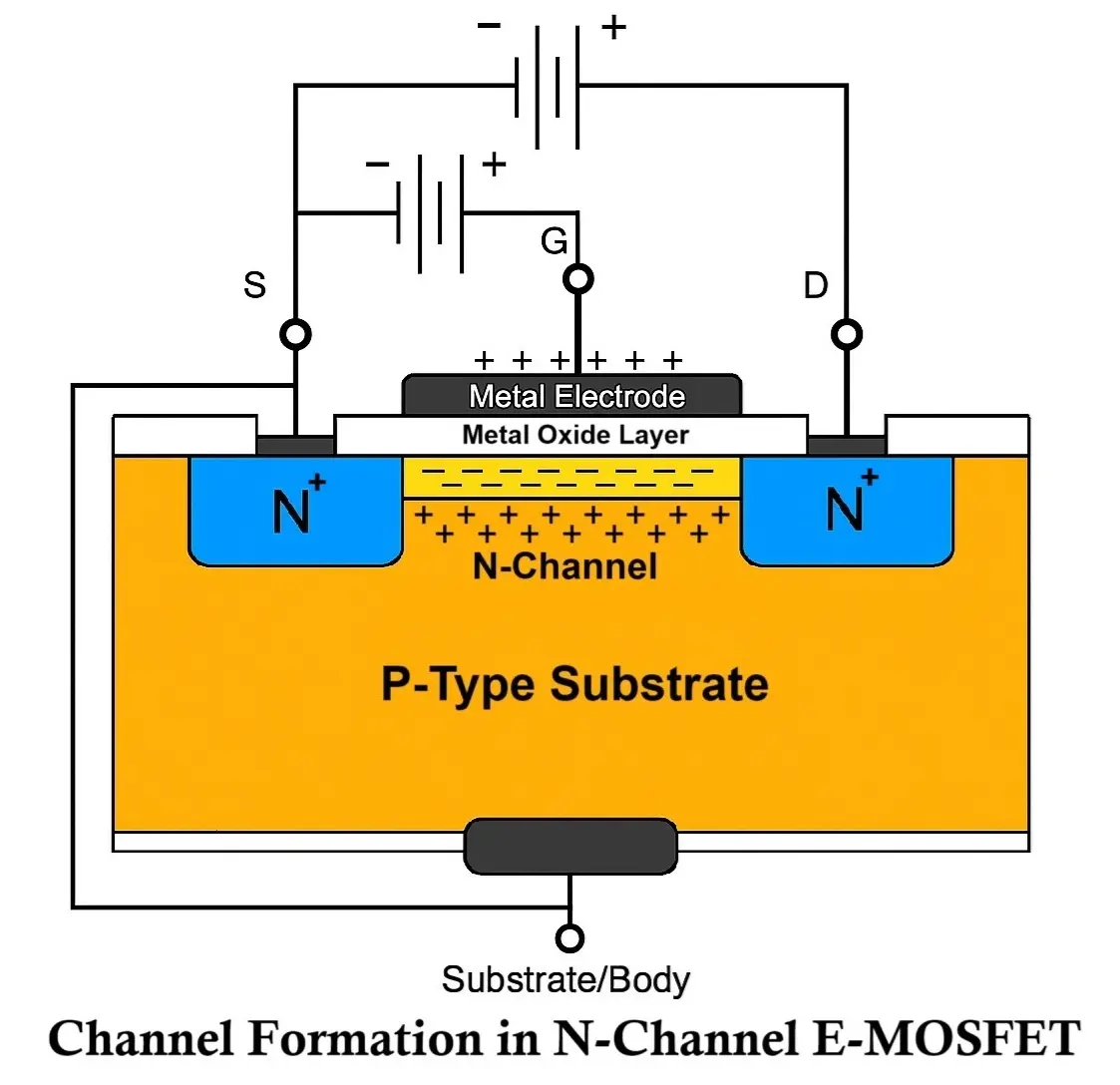
Electrons accumulate near the surface forming an inversion layer. This inversion channel later acts as the conduction path in MOSFET devices.
MOSFET as MOS Capacitor
A MOSFET gate stack is essentially a MOS capacitor. When inversion forms:
- Source and drain connect through inversion channel
- Gate capacitance controls channel charge
- Switching speed depends on gate capacitance
Flat Band Voltage
VFB = ΦMS − (Qox / Cox)
- ΦMS = metal semiconductor work function difference
- Qox = oxide charge
- Cox = oxide capacitance
Surface Potential
Strong inversion occurs when surface potential equals twice the Fermi potential:
ψs = 2ΦF
Fermi potential
ΦF = (kT/q) ln(NA / ni)
Threshold Voltage
VTH = VFB + 2ΦF + (√(2εsqNA2ΦF)) / Cox
- ΦF = Fermi potential
- εs = semiconductor permittivity
- q = electron charge
- NA = acceptor concentration
- Cox = oxide capacitance
This equation shows threshold voltage depends on oxide thickness, substrate doping, and temperature.
Capacitance Voltage Characteristics
The CV curve plots capacitance versus gate voltage and is widely used for device characterization.
- Low Frequency CV: C → Cox in strong inversion
- High Frequency CV: Minority carriers cannot respond quickly, so capacitance remains minimum in inversion.
Parameter from CV Curve
1 / C2 ∝ V
Oxide thickness:
tox = εox / Cox
Doping concentration from slope:
NA ∝ [d(1/C2)/dV]−1
Interface trap density is extracted from frequency dispersion between HF and LF curves.
Energy Band Diagram Analysis
Energy band diagrams provide physical insight:
- Accumulation: Bands bend downward.
- Depletion: Bands bend upward moderately.
- Inversion: Strong upward bending; intrinsic level crosses Fermi level.
Band bending magnitude directly equals surface potential ψs.
Frequency Response
| Region | High Frequency | Low Frequency |
|---|---|---|
| Accumulation | ≈ Cox | ≈ Cox |
| Depletion | decrease | decrease |
| Inversion | ≈ Cmin | Returns toward Cox |
Summary Table
| Region | Carrier Type | Capacitance | Band Bending |
|---|---|---|---|
| Accumulation | Majority | Maximum | Downward |
| Depletion | Ionized Dopants | Decreasing | Upward |
| Inversion | Minority | Minimum (HF) | Strong Upward |
Numerical Example
Given oxide thickness 10 nm and εox = 3.45 × 10⁻¹¹ F/m:
Cox = εox / tox = (3.45 × 10⁻¹¹) / (10 × 10−9)
Cox = 3.45 × 10⁻³ F/m2
This high capacitance enables strong gate control.
Fabrication and Practical Considerations
- Oxide thickness uniformity affects reliability.
- Fixed oxide charge shifts flat band voltage.
- Interface traps degrade subthreshold slope.
- High k dielectrics reduce leakage current.
Modern CMOS nodes below 10 nm rely heavily on optimized MOS capacitor electrostatics for performance and leakage control.
Non-Ideal Effects
- Interface trap charge causing CV stretch out
- Fixed oxide charge shifting voltage axis
- Mobile ionic charge causing hysteresis
- Oxide thickness variation reducing reliability
Advantages
- Fundamental CMOS building block
- High input impedance
- Excellent electrostatic control
- Scalable to nanometer technologies
Disadvantages
- Sensitive to oxide defects
- Thin oxide breakdown risk
- Charge trapping instability
- Frequency dependent behavior
Applications
- MOSFET channel formation
- CMOS logic gates
- DRAM charge storage
- Flash memory tunneling structures
- Semiconductor process monitoring
- Capacitive sensing technologies
Conclusion
The MOS capacitor is the electrostatic backbone of semiconductor technology. and foundation of modern electronics. Its voltage-controlled charge distribution governs MOSFET switching, CMOS scaling, and integrated circuit performance.
From Poisson equation derivation to CV characterization, it bridges device physics and practical transistor design. The CV characteristic provides deep insight into semiconductor doping, oxide quality, threshold voltage control, and interface trap density.
Types of Transistors: Classification (BJT, JFET, MOSFET & IGBT)
What is Scaling of MOSFET, Scaling Factor, and Types of Scaling
JFET Junction Field Effect Transistors Working and Applications
