Modern electronic systems rely heavily on both digital and analog signals. While microcontrollers, computers, and digital processors handle data in binary (digital form), most real-world signals such as sound, temperature, pressure, and voltage are analog. To bridge this gap, Digital to Analog Converters (DACs) are used. A DAC takes digital input (binary numbers) and converts it into a proportional analog output, usually in the form of voltage or current. Whereas Analog to Digital Converter ADC does the opposite, it converts a continuous-time, continuous-amplitude analog signal into a discrete-time, discrete-amplitude digital signal.
What is Digital to Analog Converter (DAC)?
A Digital-to-Analog Converter (DAC) is an electronic device or circuit that converts digital signals (which are discrete, binary values, usually 0s and 1s) into analog signals (which are continuous waveforms, like voltage or current that varies smoothly over time).
DACs are widely used in audio players, televisions, communication systems, instrumentation, and control systems where digital data must be represented as a continuous analog waveform.
Analog to Digital Converter (ADC) Block Diagram, Working, Types & Applications
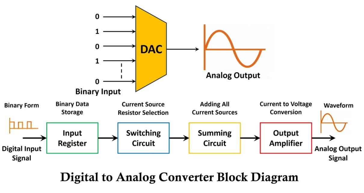
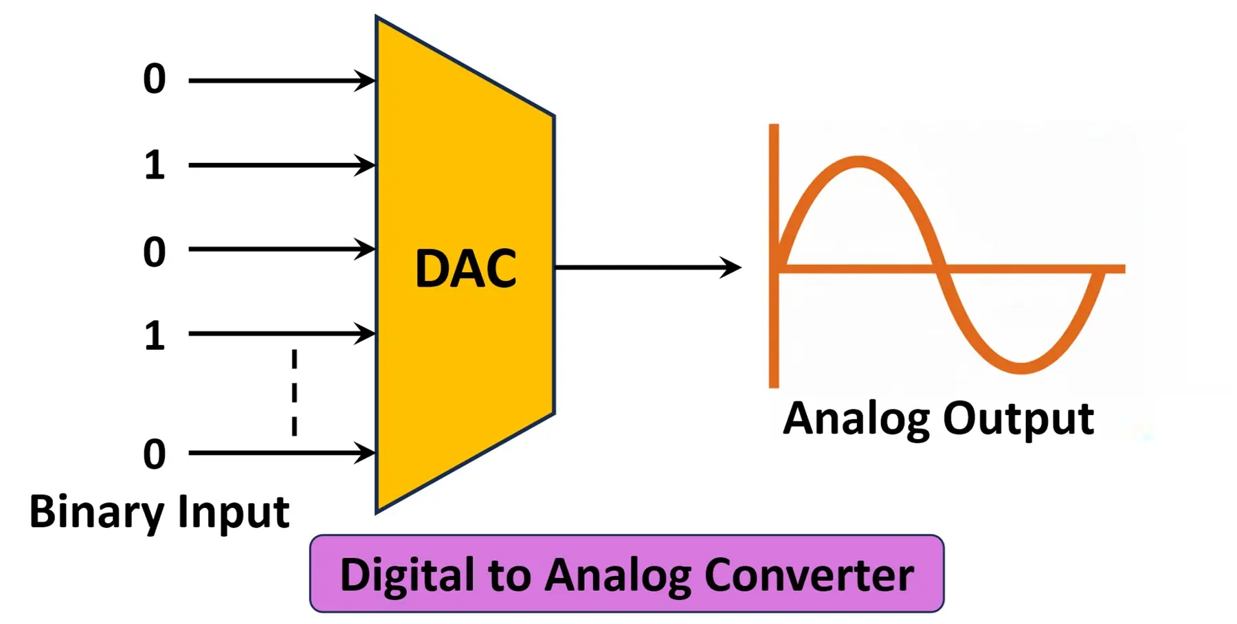
Block Diagram of Digital to Analog Converter DAC
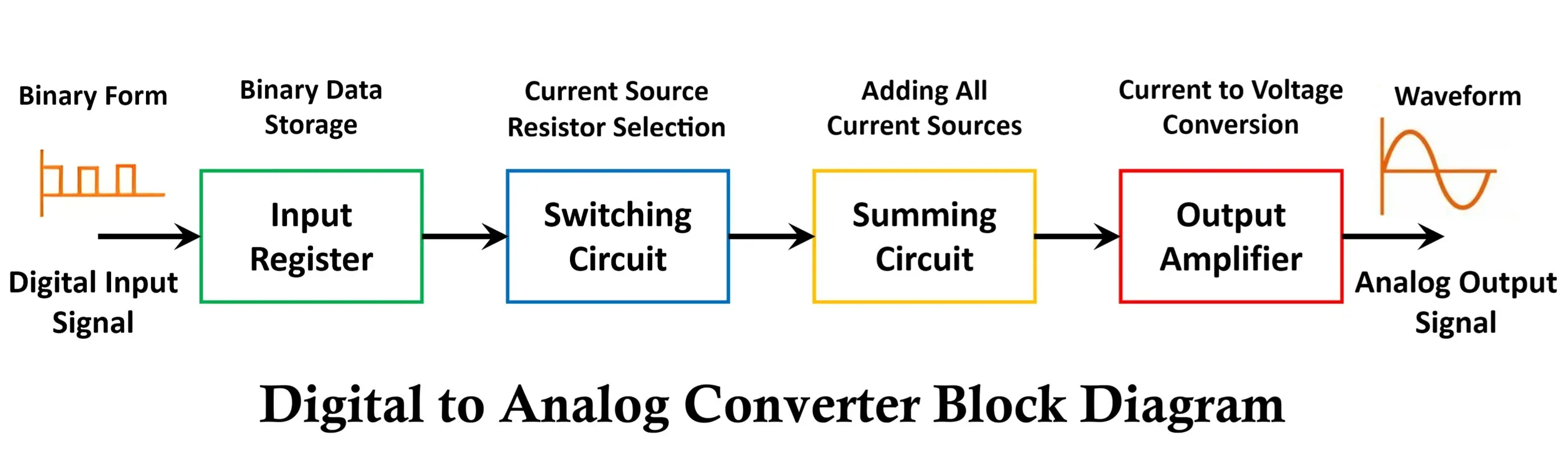
A Digital to Analog Converter converts a sequence of 1s and 0s into a continuous analog voltage or current. Let’s break down the block diagram of a DAC.
Digital Input (Binary Word)
- The input is a binary number, usually an n-bit word (e.g., 4-bit, 8-bit, 12-bit).
- Higher the number of bits → higher resolution of the DAC.
- Input is usually from a microprocessor, microcontroller, or DSP.
Digital Input Register
- Temporary storage unit for the incoming digital data (binary word).
- Ensures that all bits are applied to the DAC at the same time.
Voltage/Current Switching
- Each bit controls an electronic switch (MOSFET/transistor).
- If bit = 1 → switch connects the corresponding resistor/current source to the summing node.
- If bit = 0 → switch disconnects it (or ties to ground).
Binary Weighted Resistors / Current Sources
- The digital input bits are applied to a network of resistors or current sources.
- Each bit has a weight based on its binary position (MSB has the highest weight, LSB has the lowest).
- Two common implementations:
- Binary-weighted resistor DAC (uses resistors weighted by powers of 2).
- R-2R Ladder DAC (uses only two resistor values for simplicity).
Reference Voltage (Vref)
- Provides a stable voltage that defines the maximum analog output range.
- Acts as the “scale factor” of the DAC.
Summing Network
- The weighted outputs from resistors/current sources are summed together.
- This creates a proportional voltage/current representing the binary input.
Operational Amplifier (Op-Amp)
- Used as a summing amplifier.
- Converts the summed current into an analog voltage.
- Provides scaling and buffering so the output can drive loads.
Analog Output
- A continuous analog signal corresponding to the digital input.
- Output changes in discrete steps when the digital input changes.
- The size of each step = Resolution of the DAC.
Working of Digital to Analog Converter DAC
The working principle of a DAC can be explained in steps:
- Digital Input: The binary input (e.g., 8-bit = 00011010) is applied to the DAC through switches or logic gates.
- Resistor Network: Each bit has a weighted resistor or an R-2R network that divides the reference voltage proportionally to the bit’s significance.
- MSB (Most Significant Bit) contributes the largest portion.
- LSB (Least Significant Bit) contributes the smallest portion.
- Summing Amplifier: The weighted voltages or currents are added together.
- Analog Output: The final output is a continuous voltage or current proportional to the digital input.
Output Voltage Formula of DAC
For an n-bit DAC, the analog output voltage is:
Vout = (D / 2n) × Vref
- Vout = Analog output voltage
- D = Decimal equivalent of the digital binary input
- n = Number of bits of the DAC
- Vref = Reference voltage
Step Size (Resolution of DAC)
The smallest change in output when the digital input increases by 1 LSB (Least Significant Bit) — the step size — is:
Step Size = Vref / (2N − 1)
General Output Expression (Binary Weighted)
If the input binary code is (bn-1 bn-2 … b1 b0) (each bi is 0 or 1), the output voltage can be written as the weighted sum:
Vout = Vref × (bn-1/2 + bn-2/22 + ... + b1/2n-1 + b0/2n)
Example Calculation
For example, in an 8-bit DAC with reference voltage Vref = 5 V, the output analog voltage (Vo) can be calculated as:
- Digital input:
00011010(binary) = 26 (decimal) - Number of bits:
n = 8
Using the formula Vout = (D / 2n) × Vref:
Vout = (26 / 28) × 5
      = (26 / 256) × 5
     = 0.1015625 × 5
   = 0.5078125 V
Rounded ≈ 0.508 V
Performances Factors of Digital to Analog Converter (DAC)
Performance factors determine how accurately and efficiently a DAC converts digital signals (binary numbers) into analog voltages or currents. Let’s go through the performance factors of a Digital-to-Analog Converter (DAC) in a detailed:
1. Resolution
- Definition: Resolution is the number of distinct output levels a DAC can produce, usually expressed in bits (N-bit DAC).
- Explanation: An N-bit DAC can produce 2^N different output levels. Higher resolution means finer granularity in the output voltage.
- Impact: Determines the smallest voltage change that the DAC can produce (also called LSB – Least Significant Bit).
Formula: VLSB = VFS / (2N − 1)
Where, VFS is the full-scale voltage.
2. Accuracy
- Definition: Accuracy refers to how close the DAC output is to the ideal analog output for a given digital input.
- Factors affecting accuracy:
- Offset error: Difference between actual and expected output at zero input.
- Gain error: Deviation in slope of actual transfer function from ideal.
- Linearity error: Deviation from a straight line between output and input (includes Integral Nonlinearity (INL) and Differential Nonlinearity (DNL)).
3. Integral Nonlinearity (INL)
- Definition: INL measures the maximum deviation of the DAC’s actual output from the ideal straight-line output over the full scale.
- Significance: Affects overall linearity and accuracy; large INL can distort signals, especially in waveform generation.
4. Differential Nonlinearity (DNL)
- Definition: DNL measures how much the actual step size deviates from the ideal LSB.
- Significance:
- If DNL > 1 LSB → missing codes can occur (some digital values may not appear at output).
- If DNL < 1 LSB → smooth transition but may not be uniform.
5. Settling Time
- Definition: Time required for DAC output to reach and stay within a specified error band of the final value after a digital input change.
- Significance: Important for high-speed applications; slower settling time limits how fast the DAC can operate.
6. Monotonicity
- Definition: A DAC is monotonic if its output always increases (or stays the same) when the digital input increases.
- Significance: Essential in control systems to prevent oscillations or instability.
7. Glitch Energy
- Definition: Small unwanted voltage spikes at the DAC output during code transitions.
- Cause: Due to internal switching, especially when multiple bits change simultaneously.
- Impact: Can introduce noise in precision applications like waveform generation.
8. Output Range
- Definition: The voltage or current span that the DAC can generate (from minimum to maximum output).
- Significance: Must match the system’s required signal range; sometimes requires amplifiers.
9. Settling Error
- Definition: The difference between the ideal output and the actual output after a given settling time.
- Significance: Determines DAC’s suitability for high-speed or precision applications.
10. Output Impedance
- Definition: The resistance seen by the load connected to DAC output.
- Impact: High output impedance may interact with load and affect voltage accuracy; low output impedance is generally desired.
11. Noise and Spurious Signals
- Definition: Unwanted signals introduced by internal DAC switching or external interference.
- Significance: Reduces signal-to-noise ratio (SNR) and may limit the effective resolution of the DAC.
12. Power Consumption
- Definition: Amount of power the DAC consumes during operation.
- Significance: Important for battery-powered devices or low-power electronics.
13. Temperature Stability
- Definition: Ability of DAC performance parameters to remain consistent over temperature changes.
- Significance: Crucial for industrial, automotive, or aerospace applications.
Analog to Digital Converter (ADC) Block Diagram, Working, Types & Applications
Types of Digital to Analog Converter DAC
There are several types of Digital-to-Analog Converters DACs based on construction and working principles. Different DAC architectures have different trade-offs in speed, accuracy, complexity, and cost. Here’s a structured explanation:
1. Binary-Weighted Resistor DAC
Principle: Uses resistors weighted in powers of 2 to create a voltage proportional to the binary input.
Structure:
-
- Each bit controls a switch connected to a resistor.
- Resistor values follow R,2R,4R,8R,…R, 2R, 4R, 8R, … for LSB to MSB.
- The output voltage is a weighted sum of the input bits.
Pros:
- Simple concept
- Fast conversion speed
Cons:
- Requires precise resistor values (especially for high resolution)
- Difficult to implement for high-bit DACs due to large resistor range
Applications: Low-resolution DACs, simple circuits.
2. R-2R Ladder DAC
Principle: Uses only two resistor values, R and 2R, arranged in a ladder network.
Structure:
- Binary input switches voltage through an R-2R ladder.
- The ladder divides voltage in a way that each bit contributes a weighted amount.
Pros:
- Only two resistor values needed → easier to manufacture
- More scalable to high-bit DACs
Cons:
- Output impedance may vary, requiring buffer
- Slightly slower than some other architectures at high speed
Applications: Audio DACs, general-purpose DACs.
3. Weighted Current DAC
Principle: Uses currents instead of voltages, weighted according to the binary input.
Structure:
- Each bit controls a current source
- Currents are summed to produce an output
Pros:
- Can be integrated easily in ICs
- High speed
Cons:
- Requires accurate current sources
- More complex design than resistor DACs
Applications: High-speed communication systems, signal processing.
4. R-2R Current Steering DAC
Principle: A variant of the R-2R ladder using current sources and switches.
Structure:
- Binary-controlled switches steer currents to output
- Acts like an R-2R ladder, but in current domain
Pros:
- Very high-speed, ideal for GHz-range applications
- Good linearity
Cons:
- Requires precise matching of current sources
- Used mainly in integrated circuits
Applications: High-speed video, communication systems.
5. Resistor String DAC
Principle: Uses a series of resistors (a resistor string) and switches to select the voltage corresponding to the digital input.
Structure:
- N-bit DAC uses 2^N resistors and switches
- Output voltage corresponds to tapped resistor
Pros:
- Very linear output
- Simple concept
Cons:
- Requires many resistors → impractical for high-bit DACs
- Slow switching if many resistors
Applications: Audio DACs, instrumentation where linearity is critical.
6. Delta-Sigma (Σ-Δ) DAC
Principle: Oversamples the digital input and uses noise shaping to create a high-resolution analog output.
Structure:
- Digital input is processed by a delta-sigma modulator
- Produces a 1-bit high-frequency pulse stream
- Low-pass filter converts pulses to analog voltage
Pros:
- Very high resolution (16–24 bits)
- Excellent linearity and noise performance
Cons:
- Limited speed (not suitable for very high-frequency applications)
- Needs analog filtering
Applications: High-quality audio, measurement instruments.
7. Pulse-Width Modulation (PWM) DAC
Principle: Uses a digital pulse with varying width to represent analog values.
Structure:
- Digital signal switches a constant voltage on/off
- Low-pass filter smooths it to an analog voltage
Pros:
- Simple and inexpensive
- Easy to implement with microcontrollers
Cons:
- Requires filtering to remove ripple
- Limited resolution and speed
Applications: Motor control, microcontroller-based DACs, low-cost audio.
8. Hybrid DAC
Principle: Combines two or more DAC types to improve speed and resolution.
Example: Combining R-2R for MSBs with a resistor-string for LSBs.
Pros:
- Balances linearity, speed, and resolution
- Customizable for specific applications
Cons:
- More complex design
- Higher cost
Applications: High-performance data acquisition, instrumentation.
Advantages of Digital to Analog Converter (DAC)
High Precision and Accuracy: Modern DACs can convert digital signals to analog with very high resolution, providing precise control over the output signal.
Easy Digital Storage and Processing: Digital data is easy to store, manipulate, and transmit without degradation. The DAC converts it to analog only when needed.
Versatility: DACs can generate a wide range of analog waveforms, such as sine waves, square waves, or complex signals.
Integration with Digital Systems: DACs allow digital systems (like microcontrollers or computers) to interface with the analog world, e.g., speakers, sensors, or actuators.
Noise Immunity (During Digital Processing): Digital signals are less prone to noise and distortion compared to purely analog systems. Noise only comes into play after the DAC converts the signal.
Programmable Output: Many DACs allow software-controlled output, making them flexible for applications like signal generation and control systems.
Disadvantages of Digital to Analog Converter (DAC)
Limited Resolution: A DAC can only produce a finite number of discrete output levels. This can cause quantization error, where the analog output slightly differs from the intended signal.
Speed Limitation: The conversion speed of a DAC can limit its ability to handle high-frequency signals accurately.
Complexity: High-resolution DACs can be expensive and complex, requiring careful design for linearity, stability, and low distortion.
Analog Noise and Distortion: After conversion, the analog signal can be affected by noise, glitches, or non-linearities in the DAC, reducing signal fidelity.
Power Consumption: High-speed or high-resolution DACs often consume more power, which can be a concern in portable or low-power devices.
Cost: High-precision or high-speed DACs can be costly, especially for applications like professional audio or instrumentation.
Applications of Digital to Analog Converter (DAC)
- Audio Systems – Converting digital audio signals (MP3, CD players, smartphones) into analog signals for speakers.
- Video Systems – Digital image and video signals are converted to analog for display devices.
- Communication Systems – Used in modulation, waveform generation, and voice/data transmission over analog channels.
- Measurement & Instrumentation – Converting digital data into analog control signals for testing, calibration, and laboratory instruments.
- Control Systems – Motor speed control, robotics, industrial automation, and actuator control.
- Data Acquisition Systems – Provides analog feedback signals for displays, actuators, or monitoring systems.
- Signal Reconstruction – Restores analog signals from digital samples in digital signal processing (DSP).
- Microcontroller Applications – Generating analog outputs for sensors, actuators, and user interfaces.
- Signal Generation – Function generators, arbitrary waveform generators, and waveform synthesis.
- Medical Equipment – ECG, EEG, and other monitoring devices converting digital data to analog waveforms.
- Radar and Sonar Systems – Generating analog signals for transmission and signal processing.
- Consumer Electronics – Smartphones, tablets, digital cameras producing analog audio/video outputs.
- Musical Instruments – Digital synthesizers and electronic instruments generating analog sounds.
- Embedded Systems – Microcontroller-based analog signal output for real-world interfacing.
- Automotive Electronics – Dashboard displays, audio systems, and ECUs generating analog signals from digital data.
- Power Electronics – Analog control signals in inverters, converters, and PWM systems.
- Scientific Simulations – Analog signal simulation for experiments, labs, and testing environments.
Conclusion
A Digital to Analog Converter (DAC) is a vital component in modern electronics, acting as a bridge between digital processors and the analog world. Its block diagram typically includes a digital input register, resistor/current network, summing amplifier, and reference voltage source. Depending on the application, different architectures such as binary weighted, R-2R ladder, current steering, and sigma-delta are used. MCP4725, DFR0972 and MCP4921 are some of the popular DACs/modules often used with Arduino.
DACs play a crucial role in consumer electronics, communications, industrial automation, and audio-visual systems. With continuous advancements in semiconductor technology, DACs are becoming faster, more accurate, and more power-efficient, further expanding their applications in next-generation systems.
Analog to Digital Converter (ADC) Block Diagram, Working, Types & Applications
