An AND Gate is one of the most fundamental building blocks in digital electronics. It is a type of logic gate that performs a basic Boolean operation known as logical multiplication.
In simple terms, an AND gate produces an output only when all of its inputs are HIGH (1). If any input is LOW (0), the output becomes LOW.
AND gates play a critical role in enabling conditional decision-making and logical control across digital circuits, microprocessors, control systems, and decision-making logic.
They are essential because complex digital systems are built using combinations of simple logic gates, and the AND gate is one of the core components in this hierarchy.
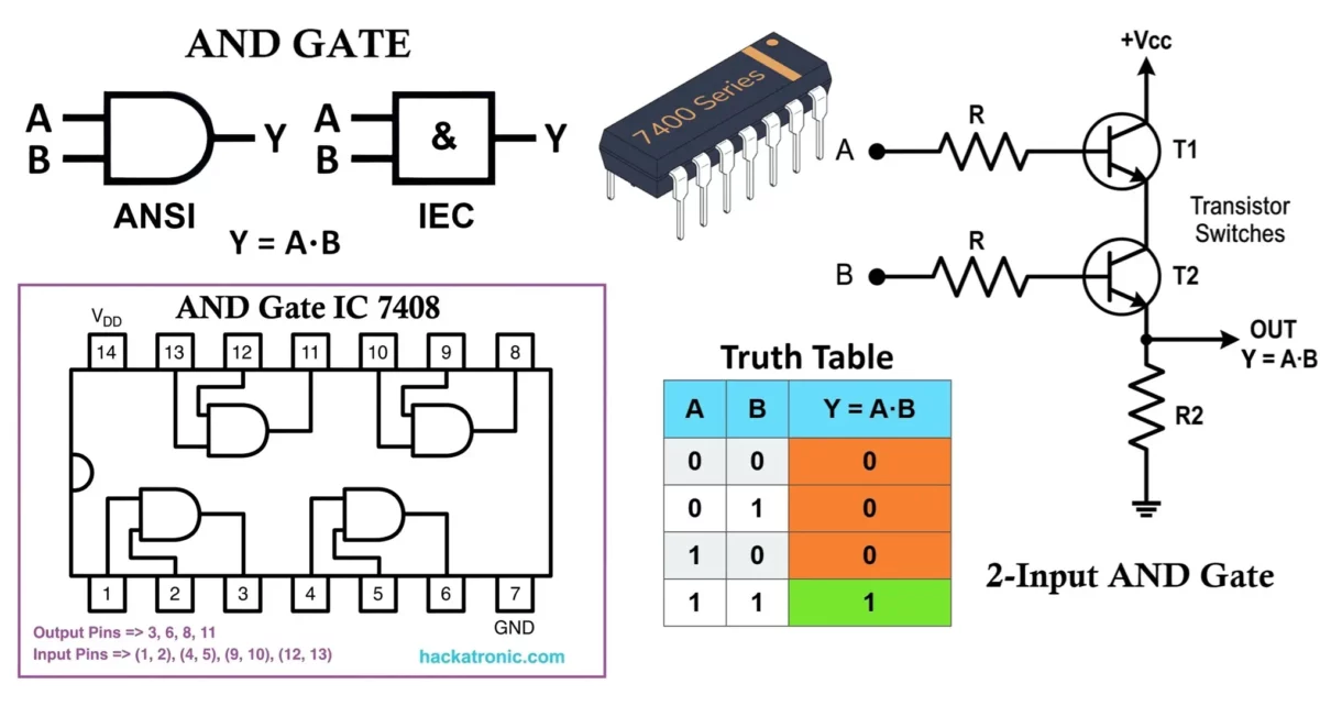
Symbol of AND Gate
- Standard Symbol (ANSI)
- The most commonly used symbol (ANSI standard) consists of:
- Flat vertical line on the left (input side)
- Semi-circular curved shape on the right (output side)
- The most commonly used symbol (ANSI standard) consists of:
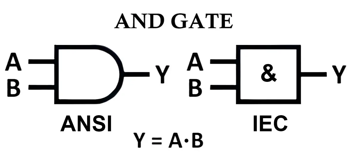
- IEC Symbol
- Represented as a rectangle
- Inside marking:
&symbol - Inputs enter from left, output exits from right
- Multi-Input Symbol
- Additional input lines are added on the left
- Output condition remains unchanged:
- Output HIGH only when all inputs are HIGH
- Terminal and Notation
- Inputs: A, B, C, D…
- Output: Y or Q
- Output is usually written as: Y = A · B
- Dot (·) represents AND operation (multiplication)
- Important Observations
- No inversion bubble → Pure AND operation
- If a bubble is added → becomes NAND gate
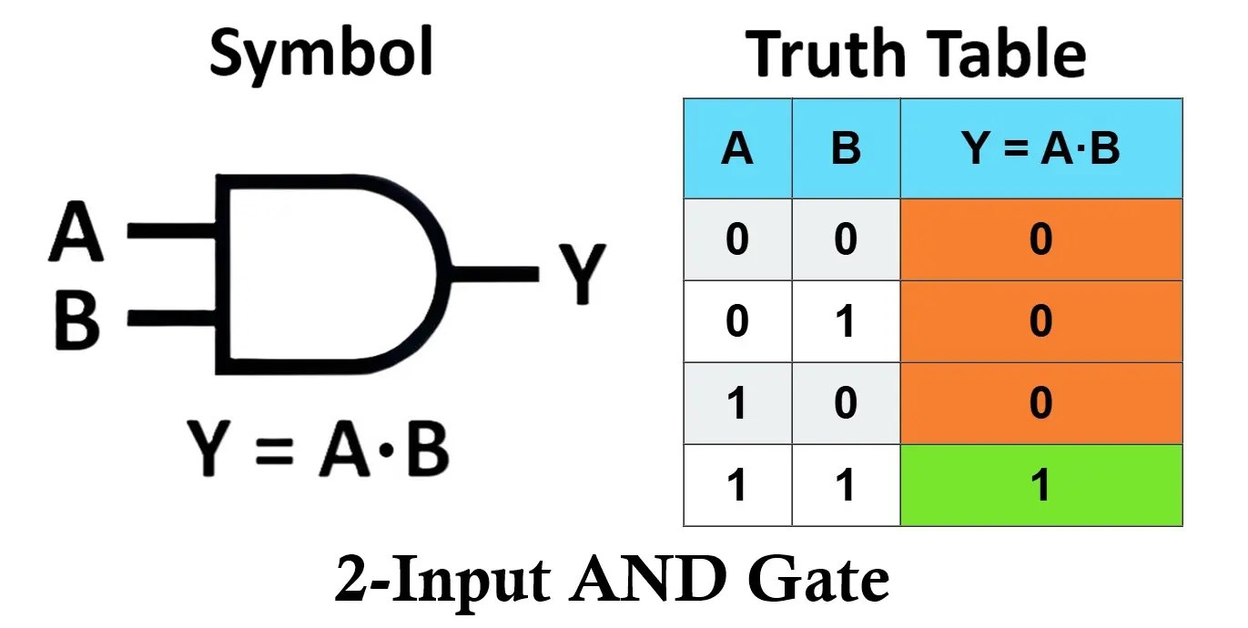
AND Gate Truth Table
- Working Principle
- The AND gate operates based on a very strict condition:
- Output is HIGH (1) only when ALL inputs are HIGH (1).
- Otherwise, the output remains LOW (0).
- Boolean Logic
- The AND operation follows Boolean multiplication rule: Y = A · B
- This is why it is called a multiplication logic gate.
- Key Condition
- ALL inputs = HIGH → Output = HIGH
- ANY input = LOW → Output = LOW
- If both A and B = 1 → Y = 1
- Otherwise → Y = 0
- This makes it highly useful in conditional logic circuits.
- Explanation
- Row 1: Both inputs LOW → Output LOW
- Row 2: One input LOW → Output LOW
- Row 3: One input LOW → Output LOW
- Row 4: Both inputs HIGH → Output HIGH
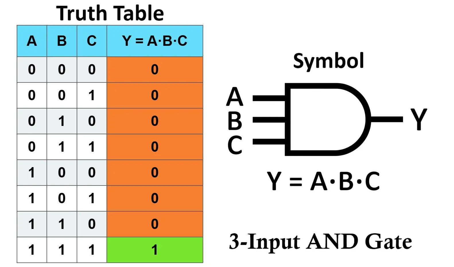
- Output is HIGH only when all three inputs are HIGH
- Extended Form: Y = A · B · C · D …
- Truth Table Insight:
- AND gate acts as a logical “permission system”
- Even one LOW input cancels the output
- Used in safety and condition-based logic
- Multi-Input AND Gates
- Can have more than 2 inputs
- Used in complex digital systems
AND Logic Circuit Implementation
Diode AND Gate (Diode Logic)
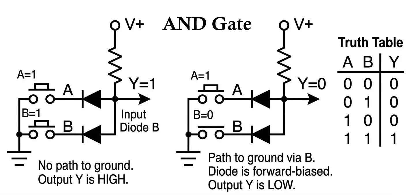
Circuit Description:
- Components
- Diodes (D1, D2)
- Resistor (pull-down)
- Working
- If any input = LOW → corresponding diode conducts → output LOW
- Only when all inputs HIGH → no conduction → output HIGH
- Limitation
- Voltage drop across diodes (~0.7V)
- Not suitable for high-speed circuits
Transistor AND Gate (RTL / TTL Concept)
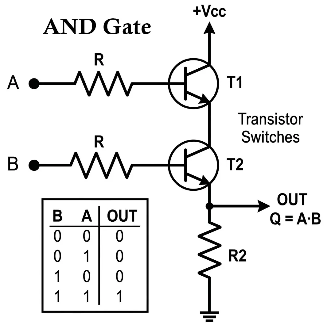
Working Principle:
- Transistors act as switches
- Connected in series configuration
- Output HIGH only when: All transistors are ON (inputs HIGH)
- If any input LOW: Corresponding transistor OFF → circuit breaks → output LOW
CMOS AND Gate
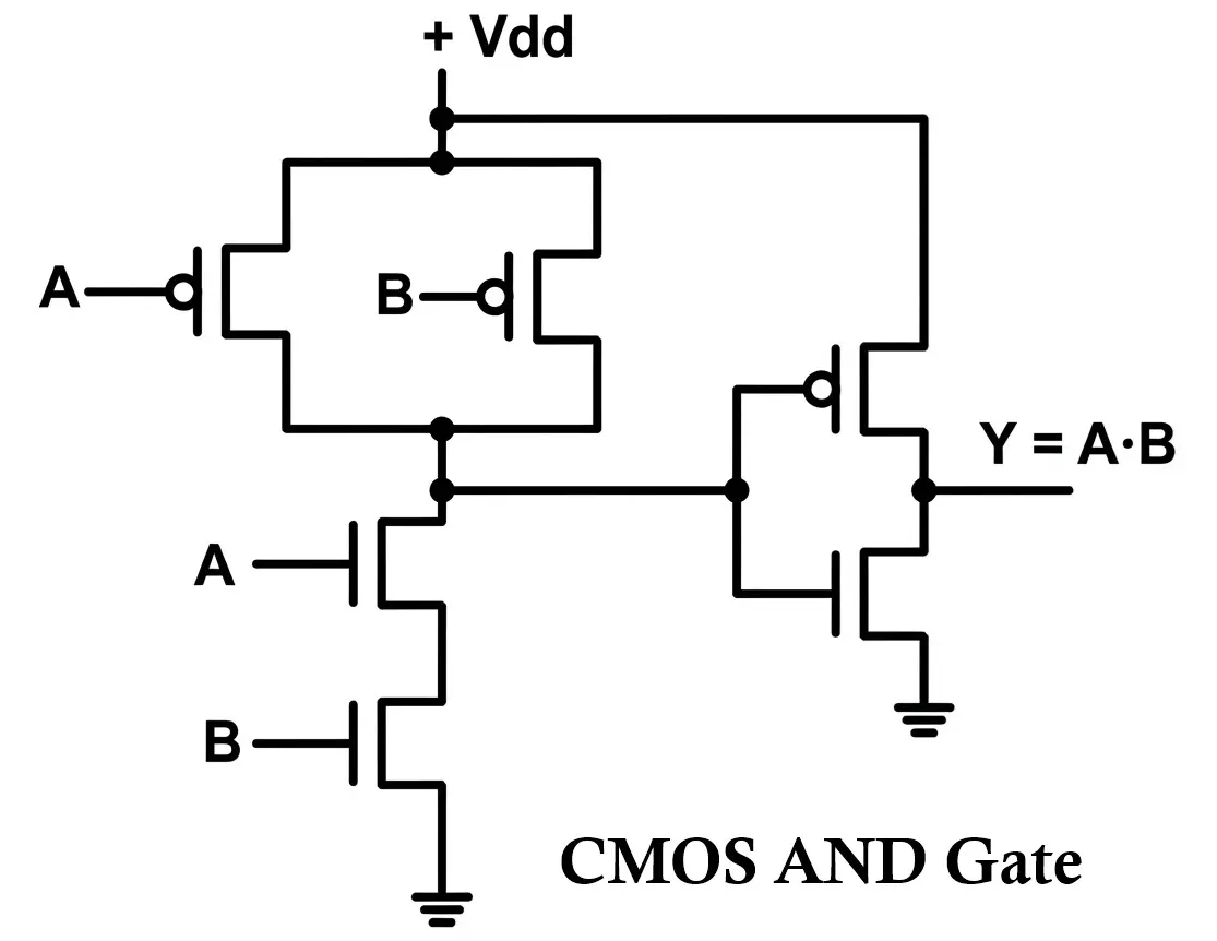
- Structure
- Uses PMOS (pull-up network)
- Uses NMOS (pull-down network)
- Configuration
- NMOS: Series → ensures AND condition
- PMOS: Parallel → complements logic
- Advantages
- Low power consumption
- High noise immunity
- Widely used in modern ICs
NAND Based AND Gate
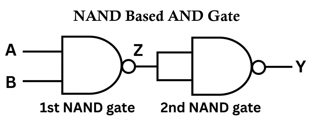
Y = (A · B) = NOT(NOT(A · B))
- One NAND for inversion
- Another NAND for logic
- NAND Gate
- NAND = NOT + AND
- Output is inverse of AND
- Y = (A · B)̅
- NAND is a universal gate (can build any circuit)
IC Numbers and Details
AND Gate IC 7408
7408 is the most popular AND Gate IC from TTL logic family.
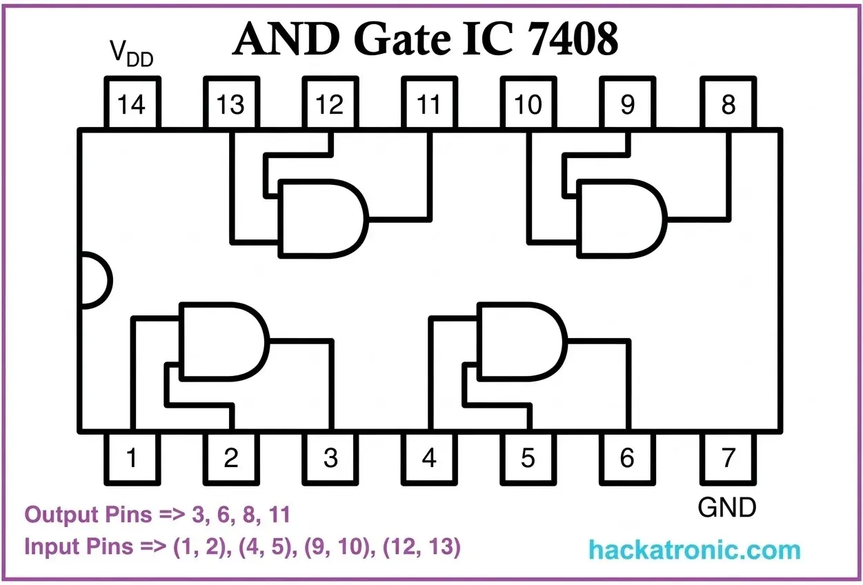
- Features
- Quad 2-input AND gates (4 gates inside)
- TTL family
- Supply voltage: 5V
- Pin Configuration
- Total pins: 14
- 4 AND gates:
- Gate1: Pins 1,2 → Output 3
- Gate2: Pins 4,5 → Output 6
- Gate3: Pins 9,10 → Output 8
- Gate4: Pins 12,13 → Output 11
- Pin 14: Vcc
- Pin 7: GND
74LS08 (Low Power Schottky)
- Faster than standard 7408
- Lower power consumption
- Widely used in digital circuits
74HC08 (CMOS Version)
- Operates at wider voltage range (2V–6V)
- Very low power consumption
- High noise immunity
74HCT08
- CMOS + TTL compatible
- Used when interfacing TTL with CMOS systems
CD4081 (CMOS)
- Quad 2-input AND gate
- Operates at 3V–15V
- Ideal for battery-operated systems
IC Comparison Table
| IC Number | Technology | Voltage | Speed | Power |
|---|---|---|---|---|
| 7408 | TTL | 5V | Medium | Medium |
| 74LS08 | TTL (LS) | 5V | High | Low |
| 74HC08 | CMOS | 2–6V | High | Very Low |
| 74HCT08 | CMOS+TTL | 5V | High | Low |
| CD4081 | CMOS | 3–15V | Medium | Very Low |
Timing and Practical Considerations
- Propagation Delay
- Time taken for output to respond
- TTL: ~10 ns
- CMOS: lower in modern ICs
- Fan-In and Fan-Out
- Fan-In: Number of inputs supported
- Fan-Out: Number of outputs driven
- Noise Margin
- CMOS > TTL
- Important for reliable operation
- Power Consumption
- TTL: Higher
- CMOS: Very low
AND Logic Example
Security System
- Consider a system with two conditions:
- Door closed (A)
- Password correct (B)
- Output (Y) = Access granted
| A | B | Y |
|---|---|---|
| 1 | 1 | 1 |
| Otherwise | → | 0 |
Access is granted only when both conditions are satisfied
Machine Control
- A machine runs only when:
- Power ON (A)
- Safety switch ON (B)
- If either condition fails → Machine stops
AND Logic Circuit Implementations
- Using Switches (Mechanical Logic)
- Series switches represent AND logic
- All switches must be closed → output ON
- Used in relay logic systems and industrial control
- Using Relay Logic
- Relays connected in series
- Output activates only when all relays energized
- Using FPGA / Digital Systems
- Implemented using HDL (Verilog/VHDL)
assign Y = A & B;
- Implemented using HDL (Verilog/VHDL)
Applications
- Logic Simplification
- Boolean algebra simplification
- Karnaugh maps (K-maps)
- Digital optimization
- In Digital Electronics
- Half Adders & Full Adders
- Multiplexers & Demultiplexers
- Encoders & decoders
- Control logic circuits
- In Computing Systems
- CPU instruction execution
- Logic decision-making
- Memory addressing
- In Everyday Electronics
- Alarm systems
- Industrial automation
- Smart home devices
Advantages
- Simple and easy to implement
- Reliable operation
- Fundamental building block
- Low cost and widely available
Limitations
- Cannot perform complex logic alone
- Requires combination with other gates
- Limited flexibility in isolation
AND Gate vs OR Gate vs NOT Gate
| Feature | AND Gate | OR Gate | NOT Gate |
|---|---|---|---|
| Boolean Expression | A · B | A + B | A̅ |
| Output Condition | All inputs HIGH | Any input HIGH | Inverts input |
| Output Behavior | Strict | Flexible | Opposite |
Key Differences
- AND Gate: Requires all conditions to be true
- OR Gate: Requires at least one condition to be true
- NOT Gate: Reverses the input logic
Conclusion
The AND gate is a fundamental component in digital electronics that performs logical multiplication. It outputs HIGH only when all inputs are HIGH, making it essential for decision-making and control logic.
Key Insights
- AND gate is a deterministic logic element
- Used in:
- Enable/disable control
- Clock gating
- Address decoding
- Essential for combinational logic design
- Multiple symbol standards (ANSI, IEC)
- Truth table defines strict logic behavior
- Implemented using:
- Diodes
- Transistors
- CMOS technology
- Available in various IC families: 7408, 74LS08, 74HC08, CD4081
- Used in both simple and complex systems
From simple circuits to complex processors, AND gates form the backbone of digital systems. Understanding their working, implementation, and applications is crucial for anyone studying electronics or designing digital circuits.
Universal NAND Gate Truth Table, Logic Circuit & IC 7400 Pin Diagram
Universal NOR Gate Truth Table, Logic Circuit & IC 7402 PIN Diagram
Types of Logic Gates with Symbol, Truth Table and IC Numbers
Classification of Digital Logic Families with Characteristics and Applications
