Photodiode is a crucial component in modern electronics, enabling devices to detect and respond to light. From remote controls and light meters to solar panels and advanced optical communication systems, photodiodes play a silent but powerful role in shaping how we interact with technology. In this article, we’ll explore everything you need to know about photodiodes, including their symbol, construction, working principle, different types, and practical applications.
What is a Photodiode?
A photodiode is a light-sensitive semiconductor device that converts light energy into electrical energy. It acts as a sensor or detector that generates a current or voltage when exposed to light, especially visible or infrared radiation. Due to this property, it is also referred to as a light sensor, photo detector, or light-dependent diode.
The principle behind a photodiode’s operation is called the photovoltaic effect—the same effect used in solar cells. When photons (light particles) strike the surface of the photodiode, they generate electron-hole pairs, resulting in an electric current that is directly proportional to the intensity of the light.
A real-world example of this effect is a solar cell, which is essentially a large array of photodiodes (or photovoltaic cells) designed to convert sunlight into usable electric power.
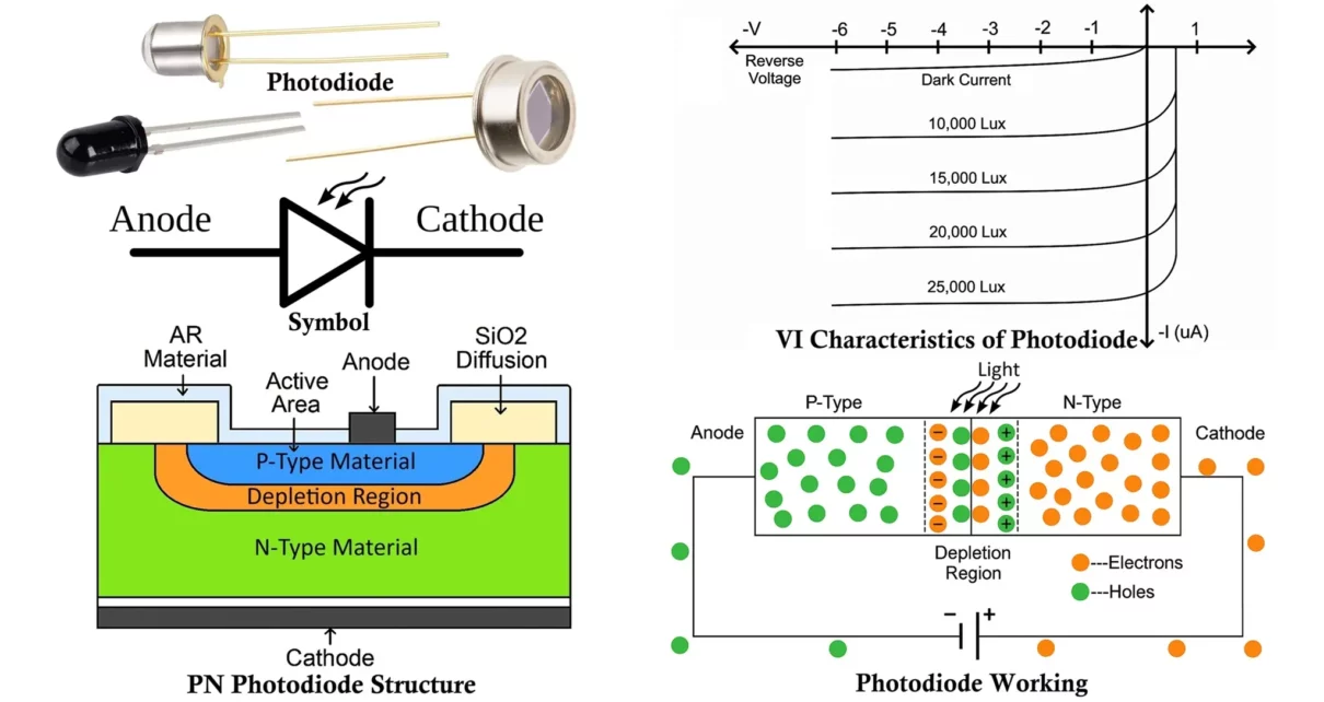
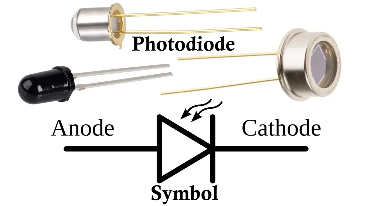
Symbol of Photodiode
The standard circuit symbol of a photodiode resembles that of a regular diode, but with two arrows pointing toward the junction, representing incoming light:
- Anode (P-side): Typically connected to the negative terminal (reverse bias)
- Cathode (N-side): Typically connected to the positive terminal
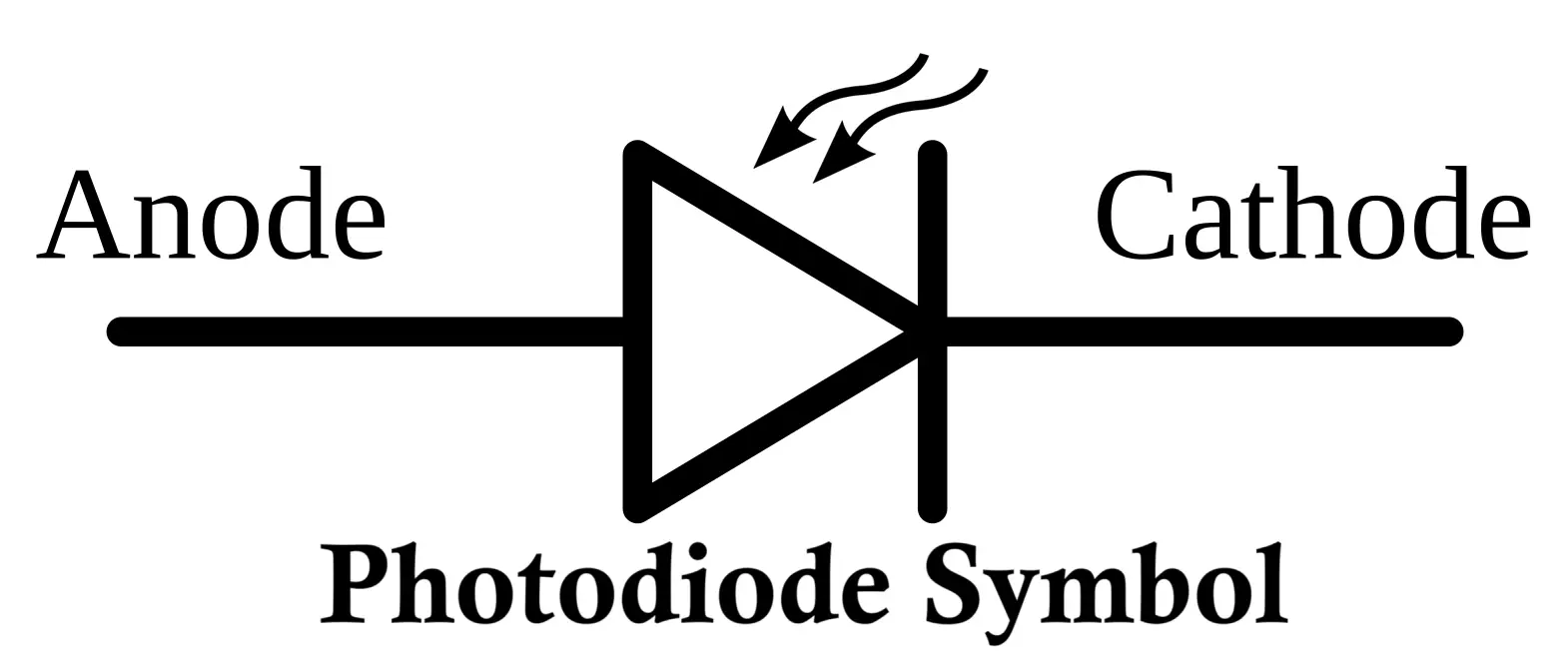
This symbol clearly indicates that the device is light-sensitive and works when exposed to light.
Construction of Photodiode
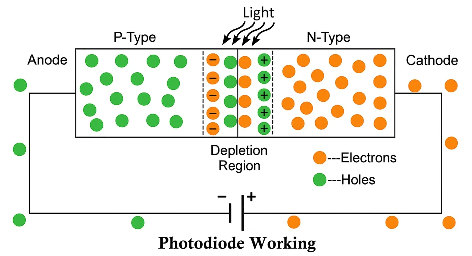
The basic construction of a photodiode centers around the PN junction, which is the heart of the device. It is formed by joining two types of semiconductor materials: P-type and N-type. This junction is carefully engineered to ensure high sensitivity to light while minimizing unwanted electrical interference.
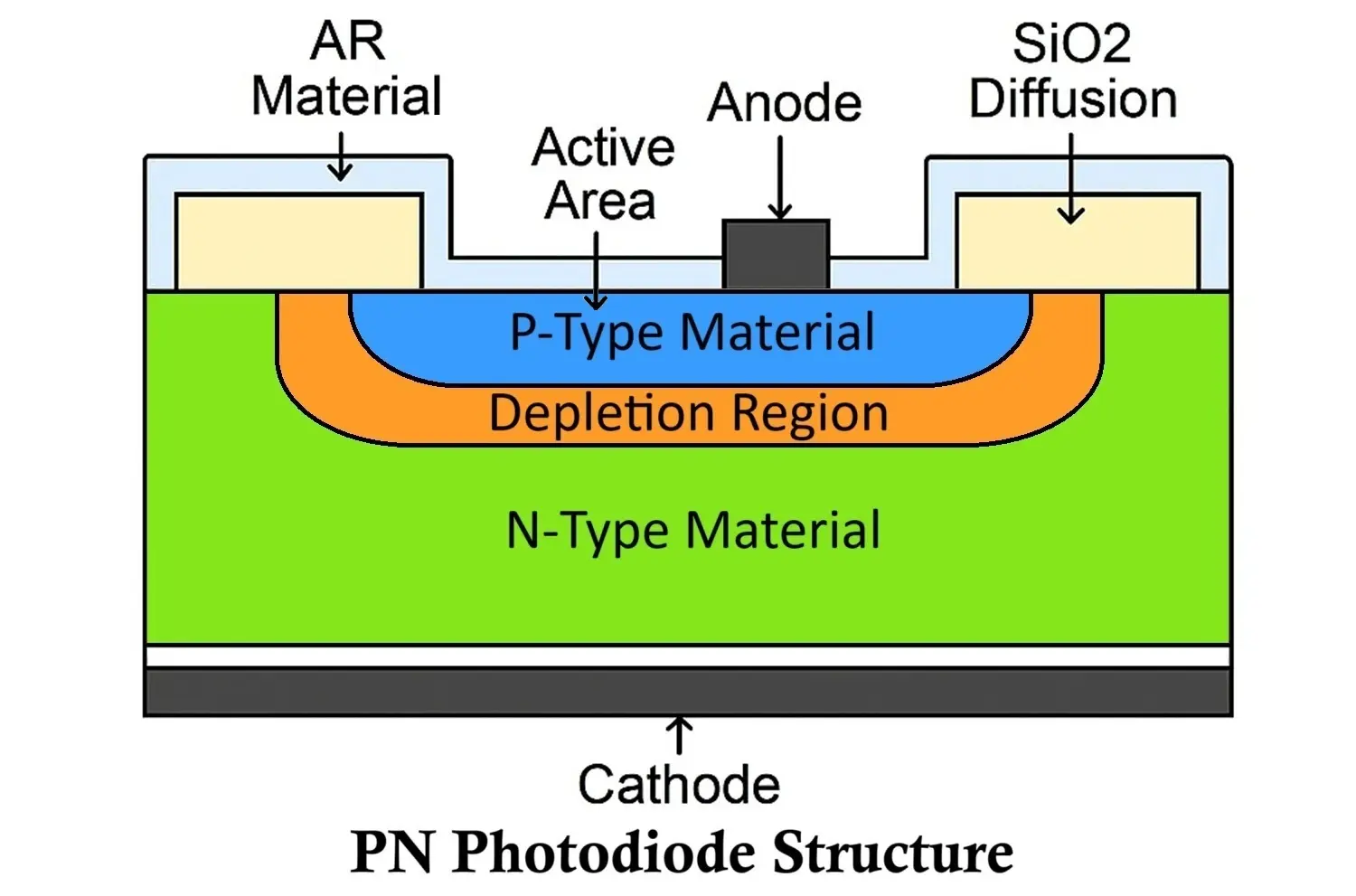
Cross-Sectional Structure
A typical photodiode consists of:
- A lightly doped P-type semiconductor layer
- A heavily doped N-type semiconductor layer
- A depletion region formed at the junction where no free charge carriers exist
When these layers are joined, electrons from the N-region combine with holes from the P-region, forming a depletion layer that acts as a barrier to charge movement. This region possesses a built-in electric field, which is crucial for separating the electron-hole pairs generated by incoming photons. It allows current to flow in only one direction when the photodiode is reverse biased or operated under photovoltaic mode.
Light Collection and Optical Layering
- The photodiode’s active region is exposed to light through a glass window or lens, which focuses and collects more light to improve efficiency.
- An anti-reflective (AR) coating maximizes photon absorption by reducing reflection.
- Non-active areas are shielded with black paint or a SiO₂ metalized layer to block stray light and prevent leakage current.
Terminals and Contacts
- The cathode and anode terminals are connected via metal contacts.
- The anode is connected to the P-layer, and the cathode is connected to the N-layer.
- These terminals allow the photodiode to be integrated into external circuits.
Working of Photodiode
The working principle of a photodiode is closely related to that of a standard PN junction diode, but it is designed to respond to light.
Photodiode in Reverse Bias
Photodiodes are typically operated under reverse bias or sometimes under zero bias (not in forward bias). When a PN junction diode is reverse biased:
- The depletion region widens
- A small reverse current flows due to minority charge carriers
- This current is normally very low and depends on the reverse voltage applied
Generation of Photocurrent
In a photodiode, the situation changes dramatically when light enters the picture. When a photon (a particle of light) with energy greater than or equal to the bandgap energy (hv ≥ Eg) strikes the depletion region of the photodiode, it provides enough energy to excite an electron from the valence band to the conduction band.
This process creates:
- A free electron
- A corresponding hole in the valence band
Together, they form an electron-hole pair – the key to generating current in the photodiode. This phenomenon is known as the inner photovoltaic effect.
Movement of Charge Carriers
Thanks to the built-in electric field across the depletion region:
- Electrons are pulled toward the N-side (cathode)
- Holes are pulled toward the P-side (anode)
This separation of charge carriers creates a current called the photocurrent.
The magnitude of this photocurrent is directly proportional to the intensity of the incident light. More light = more photons = more electron-hole pairs = higher current.
Dark Current
Even in the absence of light, a small amount of current still flows through the photodiode. This is known as the dark current.
- Caused by thermally generated charge carriers
- Usually in the range of microamperes (µA)
- Considered undesirable, as it adds noise and limits the sensitivity of the photodiode
Dark current increases with temperature and must be minimized in precision applications like light meters or medical instruments.
Total Output Current
The total current flowing through a photodiode is given by:
Itotal = Iphoto + Idark
Where:
- Iphoto is the useful photocurrent generated by incident light
- Idark is the unwanted leakage or dark current
For accurate light sensing, reducing dark current is essential so that the output reflects only the true intensity of the incoming light.
Operating Modes of Photodiode
Photodiodes can operate in three different modes, depending on how they are biased and what type of circuit they are used in.
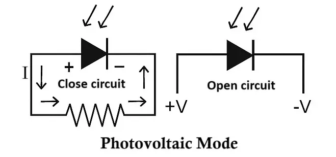
1. Photovoltaic Mode (Zero Bias Mode)
In Photovoltaic Mode, the photodiode operates without any external bias—hence the name Zero Bias Mode. It relies solely on the built-in electric field of the PN junction to separate the electron-hole pairs generated when photons strike the depletion region.
Key Features:
- No external power supply is required
- Generates a voltage (in open circuit) or a current (in closed circuit) when exposed to light
- The voltage across the terminals is forward-biased as light intensity increases
Operation:
- In open-circuit conditions, a voltage develops across the anode and cathode, proportional to the light intensity.
- In closed-circuit conditions, a small forward current flows, equal to the sum of photocurrent and dark current.
Limitations:
- Nonlinear output
- Low dynamic range
- Slow response time due to high junction capacitance
- Best suited for low-frequency, low-light applications
Applications:
- Solar cells
- Low-light sensors
- Battery-less light meters
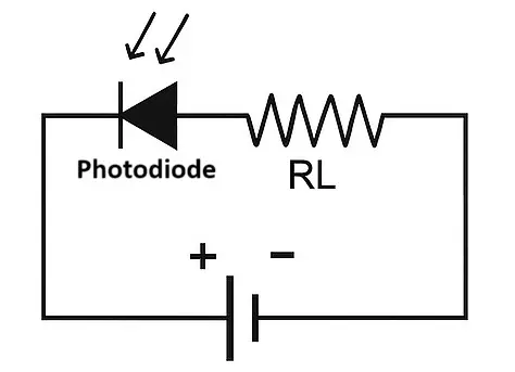
2. Photoconductive Mode (Reverse Bias Mode)
In Photoconductive Mode, the photodiode is operated under reverse bias. The anode is connected to the negative terminal, and the cathode is connected to the positive terminal of the power supply. This mode is commonly used for high-speed and accurate light sensing.
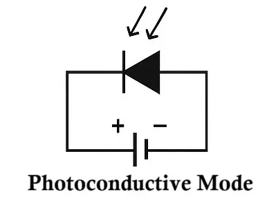
Key Features:
- Depletion region widens with reverse bias
- Capacitance decreases, improving response time
- Suitable for high-speed and high-frequency applications
Operation:
- When light hits the depletion region, electron-hole pairs are generated.
- The external reverse voltage helps in quick separation and collection of these charge carriers.
- Generates a larger photocurrent due to the increased efficiency of carrier movement.
Side Effect – Dark Current:
- Even without light, a small reverse leakage current (dark current) flows.
- Increases with temperature and adds electrical noise
- Must be minimized in sensitive applications
Applications:
- Fiber-optic communication
- Barcode scanners
- Optical encoders
- IR receivers
3. Avalanche Mode (High Reverse Bias)
In Avalanche Mode, the photodiode is subjected to a very high reverse bias voltage—close to or beyond its breakdown voltage. This triggers a chain reaction of impact ionization, greatly amplifying the generated photocurrent.
Key Features:
- High internal gain (amplified photocurrent)
- Extremely high sensitivity
- Operates using the avalanche multiplication effect
Operation:
- Photons striking the depletion region generate electron-hole pairs.
- These carriers accelerate under the high electric field, gaining enough energy to ionize other atoms, creating more carriers.
- This avalanche effect results in significant current amplification.
Limitations:
- Requires complex circuitry for stable operation
- Generates more noise than other modes
- Higher power consumption
Applications:
- Low-light level detection
- Medical imaging
- LIDAR systems
- Photon counting systems
Each of these three modes is tailored for specific needs – from energy harvesting and ambient light sensing to high-speed optical detection.
A photodiode alone cannot power electronic devices because the current it produces is extremely small. Therefore, an external power source is required to boost the current delivered to the load.
Quantum Efficiency of Photodiode (QE)
- Definition:
Quantum efficiency (QE) measures how well a photodiode converts incoming photons (light) into electrons (electric current). - Basic Formula:
QE = (Number of electrons generated / Number of incident photons) × 100
- Meaning:
A higher QE means more of the incoming light is being used to generate current – better efficiency. - Wavelength Dependence:
QE depends on the wavelength (color) of light. Some wavelengths are absorbed more effectively than others. - Anti-Reflection Coating:
Special coatings are applied to reduce light reflection at the surface, allowing more photons to enter and increasing QE. - Typical Value:
QE can reach up to 95% for well-optimized photodiodes at certain wavelengths. - Relation to Responsivity:
QE is directly related to the photodiode’s responsivity (R), which is the electrical current output per unit of light power (A/W).
Formula Linking QE and Responsivity:
QE = (R⋅h⋅c)/(q⋅λ)
where:
- R = Responsivity (A/W)
- h = Planck’s constant
- c = Speed of light
- q = Electron charge
- λ = Wavelength of light (in meters)
Performance Parameters of Photodiode
The performance and efficiency of a photodiode are determined by several key parameters. These parameters help evaluate how well a photodiode will respond to light, how quickly it can react, and how much noise it introduces into the system. Understanding these factors is essential when selecting a photodiode for a specific application.
1. Response Time
Response time refers to the time it takes for charge carriers (electrons and holes) generated by incident light to cross the depletion region of the photodiode and contribute to the output current.
- It is directly influenced by the junction capacitance of the diode.
- Wider depletion regions (achieved through reverse biasing) result in lower capacitance, which leads to faster response times.
- Faster response time is critical in high-speed applications like fiber-optic communication or optical switching.
2. Responsivity
Responsivity is a measure of how effectively a photodiode converts incident optical power into electrical current. It is defined as:
Responsivity = Photocurrent (A) / Incident Optical Power (W)
- Unit: Amps per Watt (A/W)
- It depends on the wavelength of the incident light and the material of the photodiode.
- Higher responsivity indicates greater sensitivity, meaning more current is generated for a given amount of light.
3. Dark Current
Dark current is the small current that flows through a photodiode even in complete darkness when it is reverse biased.
- Analogous to leakage current in regular diodes
- Typically measured in microamperes (µA)
- Increases with temperature
- Unbiased (photovoltaic mode) photodiodes generally exhibit lower dark current
Though dark current is usually very small, it contributes to electronic noise and can reduce the accuracy of low-light measurements. It becomes especially significant in precision and low-signal applications.
4. Breakdown Voltage
Breakdown voltage is the maximum allowable reverse voltage that can be applied to a photodiode before it enters avalanche breakdown.
- Exceeding this limit causes a rapid increase in reverse current, potentially damaging the device permanently.
- Breakdown voltage varies with temperature and tends to decrease as temperature increases.
Operating below the breakdown threshold ensures long-term stability and safe performance of the photodiode.
VI Characteristics of Photodiode
The Voltage-Current (VI) characteristics of a photodiode illustrate how the current through the device varies with applied voltage under different lighting conditions. These characteristics are crucial in understanding the behavior and sensitivity of the photodiode in various operating environments.
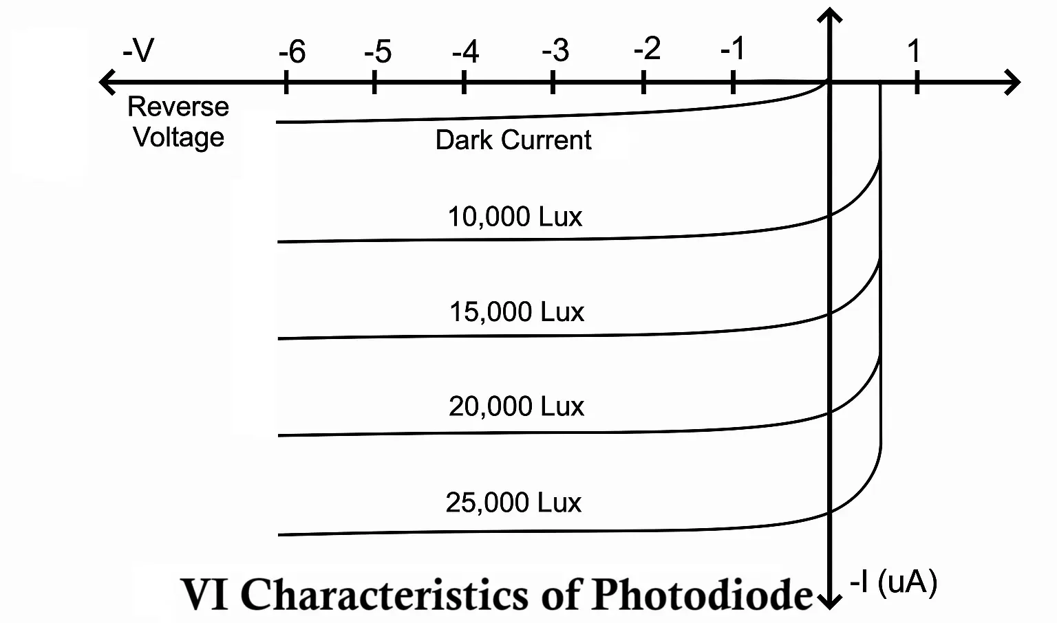
Understanding the VI Curve
The VI characteristics curve of a photodiode is typically plotted with:
- Voltage (V) on the horizontal axis (X-axis)
- Current (I) on the vertical axis (Y-axis)
Since photodiodes are designed to operate in reverse bias, the graph focuses on the negative voltage region (left side of the X-axis) and the reverse current (downward side of the Y-axis, in microamperes).
Behavior in Reverse Bias
- When no light is falling on the photodiode, only a small constant reverse current flows – this is known as the dark current.
- As the intensity of incident light increases, more electron-hole pairs are generated, leading to a higher reverse photocurrent.
- This reverse current increases linearly with light intensity but remains mostly independent of the reverse voltage, as long as the diode is below its breakdown voltage.
VI Characteristics Curve Summary
- At zero light, only the dark current flows.
- As light intensity increases, the curve shifts downward, indicating an increase in reverse current.
- Photocurrent is nearly constant for a given light intensity across a range of reverse voltages, showing that light—not voltage—is the main driver of current change.
- Forward bias region is rarely used, as it introduces large current and defeats the purpose of light sensing.
Graphical Representation
If plotted, the VI characteristic curves for different light levels would appear as a set of parallel reverse current lines, each lower (more negative) as light intensity increases:
The VI characteristics confirm the linear relationship between light intensity and reverse current, making photodiodes highly effective for accurate and fast photo-detection in various electronic and optical systems.
Types of Photodiodes
Although all photodiodes operate on the same fundamental principle – converting light into electrical current, there are various types, each tailored to enhance specific parameters such as speed, sensitivity, or noise reduction. The most commonly used photodiodes include:
1. PN Photodiode
The PN photodiode is the most basic and earliest form of photodiode, consisting of a single PN junction, much like a conventional diode.
Features:
- Operates under reverse bias
- Small depletion region that expands with increased reverse voltage
- Low response time and lower sensitivity
- Simple structure and low cost
However, the reverse bias that improves depletion width also increases dark current, which adds unwanted electrical noise. Due to these limitations, PN photodiodes are now largely replaced by more advanced types like the PIN photodiode.
2. PIN Photodiode
The PIN photodiode is a highly efficient improvement over the PN photodiode. It introduces an intrinsic (I) semiconductor layer between the P-type and N-type materials, forming a P-I-N structure.
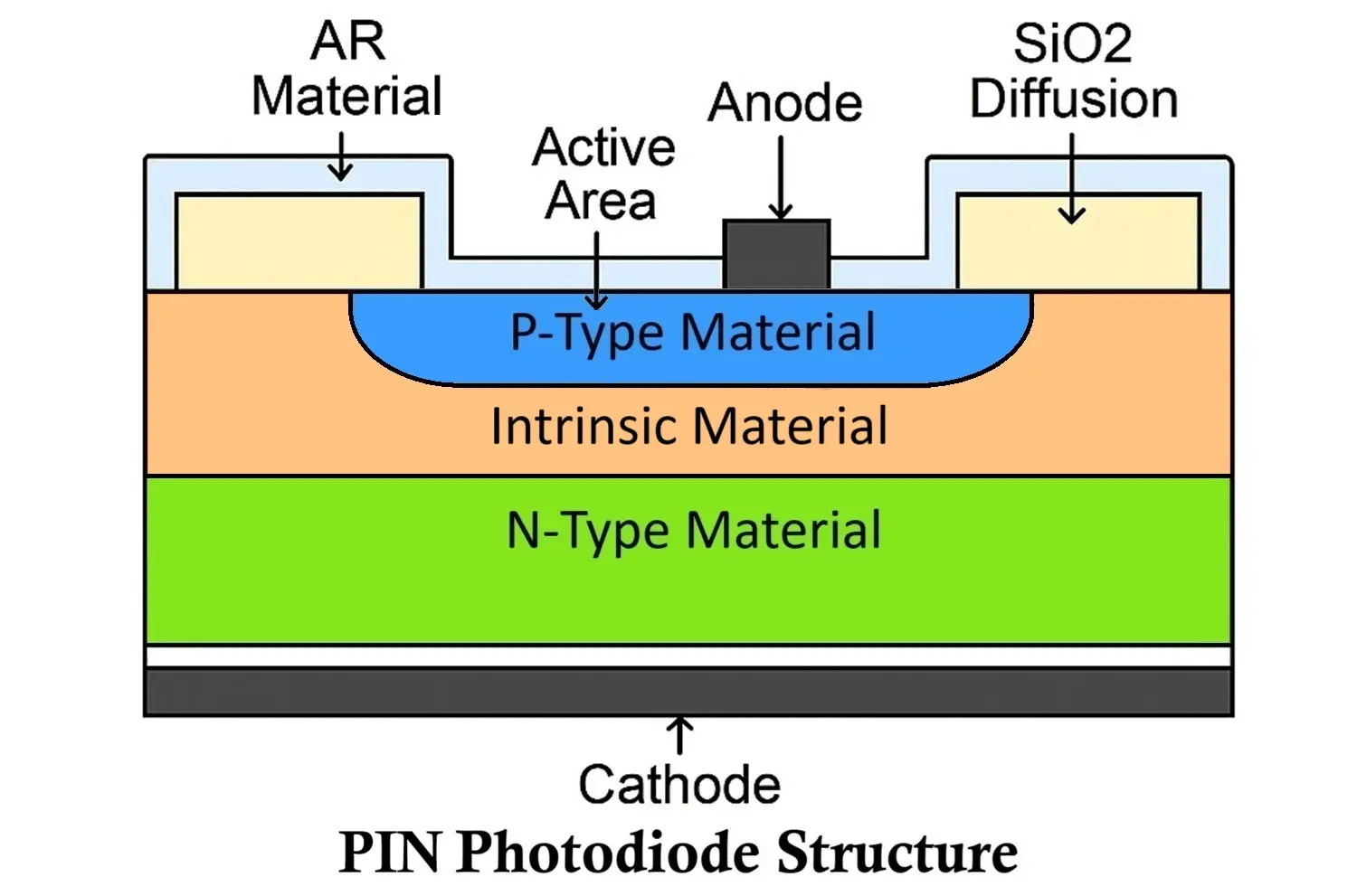
Structure:
- P-type layer (anode)
- Intrinsic layer (light-sensitive region)
- N-type layer (cathode)
The intrinsic region increases the depletion width and active area, improving sensitivity, speed, and bandwidth.
Working:
- Light strikes the intrinsic layer, generating electron-hole pairs
- Reverse bias widens the depletion region, enabling quick collection of carriers
- Electrons move toward the N-layer, holes toward the P-layer
Advantages:
- Higher sensitivity than PN photodiode
- Faster response time
- Lower junction capacitance
- Suitable for high-frequency applications
- Wider bandwidth
Used in optical communication, laser detection, and high-speed light sensors
PIN Diode Symbol, Construction, Working & Applications
3. Avalanche Photodiode
The Avalanche Photodiode (APD) is a specialized type designed for high internal gain through a process known as impact ionization or avalanche multiplication.
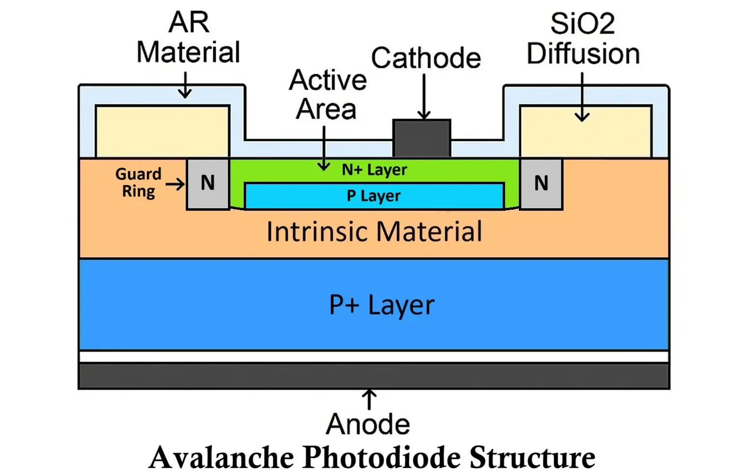
Structure:
- Multi-layered (P⁺, I, P, N⁺)
- Guard ring to prevent edge breakdown
- Operates under very high reverse bias
Working:
- Photons generate electron-hole pairs
- High reverse voltage causes carriers to accelerate and collide with atoms
- Each collision generates more carriers, amplifying the photocurrent
Advantages:
- Very high sensitivity
- Can detect very low-intensity light
- High signal gain
- Fast response time
- Better Signal-to-Noise Ratio (SNR)
Limitations:
- Requires high reverse voltage
- Generates electrical noise
- Temperature-sensitive (often requires heat sinks)
Ideal for LIDAR, photon counting, medical imaging, and low-light detection
Avalanche Diode Symbol, Construction, Working & Applications
4. Schottky Photodiode
The Schottky photodiode (also called Metal-Semiconductor (MS) photodiode) uses a metal-semiconductor junction instead of a traditional PN or PIN structure.
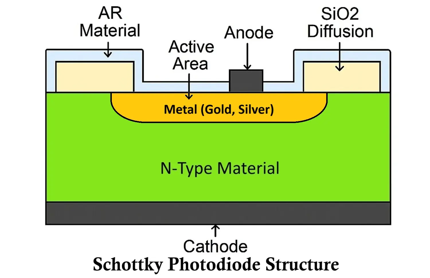
Structure:
- Transparent metallic layer (e.g., gold) over an N-type semiconductor
- No P-type material involved
Working:
- Incident light passes through the metal and enters the semiconductor
- Photon energy releases electron-hole pairs in the depletion region
- The built-in electric field sweeps carriers to generate photocurrent
Advantages:
- Extremely fast response (up to 50 GHz)
- Excellent for short-wavelength and high-frequency applications
- No ohmic contacts required
- Compact and reliable
Used in ultrafast photodetectors, microwave optical systems, and telecommunications
Schottky Diode Symbol, Construction, Working & Applications
Comparison Table
| Type | Speed | Sensitivity | Noise Level | Operating Voltage | Common Applications |
|---|---|---|---|---|---|
| PN Photodiode | Low | Low | Low | Low | Basic light sensors |
| PIN Photodiode | High | High | Moderate | Moderate to High | Optical communication, IR sensors |
| Avalanche Photodiode | Very High | Very High | High | Very High | LIDAR, photon counting, medical imaging |
| Schottky Photodiode | Ultra High | Moderate | Low | Low to Moderate | GHz-range detection, ultrafast switching |
Each photodiode type has its unique strengths, making it suitable for specific use-cases depending on speed, light intensity, frequency, and circuit complexity.
Advantages of Photodiode
Photodiodes offer several benefits that make them essential in modern technology:
- Light-powered operation – Works directly using light energy without requiring complex conversion processes.
- High-speed communication – Ideal for fast data transfer in optical fiber networks.
- Low noise generation – Produces minimal interference during signal processing.
- Low dark current – Generates less unwanted current in the absence of light compared to phototransistors.
- High quantum efficiency – Converts a large portion of incoming photons into electrical signals.
- Low internal resistance – Enhances signal transmission efficiency.
- Durable and long-lasting – Rugged construction ensures extended operational life.
- Low voltage requirement – Operates efficiently on minimal voltage supply.
- Linear output – Provides a consistent response to varying light intensities.
- Economical – Cost-effective to manufacture and deploy.
Disadvantages of Photodiode
Despite its benefits, the photodiode has a few limitations:
- Small active area – Limited surface area for light detection.
- Lower sensitivity – Not as responsive as certain other light-sensing components.
- External power dependency – Needs an external source to drive sufficient current to the load.
- Requires amplification – Additional circuitry needed for low-light conditions.
- Slow in basic forms – Standard PN photodiodes have a higher response time.
- Thermal noise interference – Heat can reduce performance accuracy.
- Poor temperature stability – Sensitive to environmental temperature changes.
- Offset voltage requirement – Needs a bias voltage for optimal functioning.
Applications of Photodiode
Since photodiodes detect and measure light intensity, their use spans across multiple industries and technologies.
1. Electrical Isolation
Used in optocouplers to separate low-voltage sensitive circuits from high-voltage ones, ensuring safe signal transfer through optical means without direct electrical connection.
2. Renewable Energy
Key components in solar panels, converting sunlight into usable electricity for both domestic and industrial purposes. Solar plants often use thousands of photodiodes arranged in panels.
3. Optical Communication
High-speed photodiodes, such as PIN types, are essential for transmitting data through fiber optic cables in telecommunication systems.
4. Building Safety Systems
Integrated into smoke and fire alarms, photodiodes detect smoke particles via light interruption, triggering early warnings.
5. Medical Equipment
Used in advanced imaging and diagnostic tools like CT scanners, PET scanners, and laboratory analyzers.
6. Security Devices
- Burglar alarms – Detects interruptions in a steady light beam to trigger security alerts.
- Object counters – Counts items by detecting when light is blocked.
7. Everyday Electronics
- Light sensors in digital cameras for exposure control.
- Detection of both visible and invisible (IR) light.
- Optical encoders and decoders for precise motion control.
- Proximity sensors and barcode readers.
- Automatic streetlights that switch based on light levels.
- Infrared remote controls for TVs, air conditioners, and more.
- CD players, scanners, and printers for tracking media or paper movement.
- Variable resistance devices for light-sensitive control circuits.
- High-speed digital logic systems due to their low voltage and quick response.
- Character recognition systems in automated processing.
Conclusion:
Photodiodes strike a balance between efficiency, cost-effectiveness, and versatility. While they may require additional circuitry in low-light conditions and have some thermal limitations, their role in renewable energy, communication, safety, and everyday electronics ensures they remain a cornerstone of modern optoelectronic technology. Vishay BPW21R, Vishay BPW34, Hamamatsu S1087, Hamamatsu S1133, Hamamatsu S1133-01, Hamamatsu S1133-14, Hamamatsu S8664, Thorlabs SM05PD3A are some of the popular Photodiode series.
Types of Diodes with Symbol, Definition, Working and Applications
Definition of Diode, VI Characteristics, Working and Application
Types of Transistors: Classification (BJT, JFET, MOSFET & IGBT)
