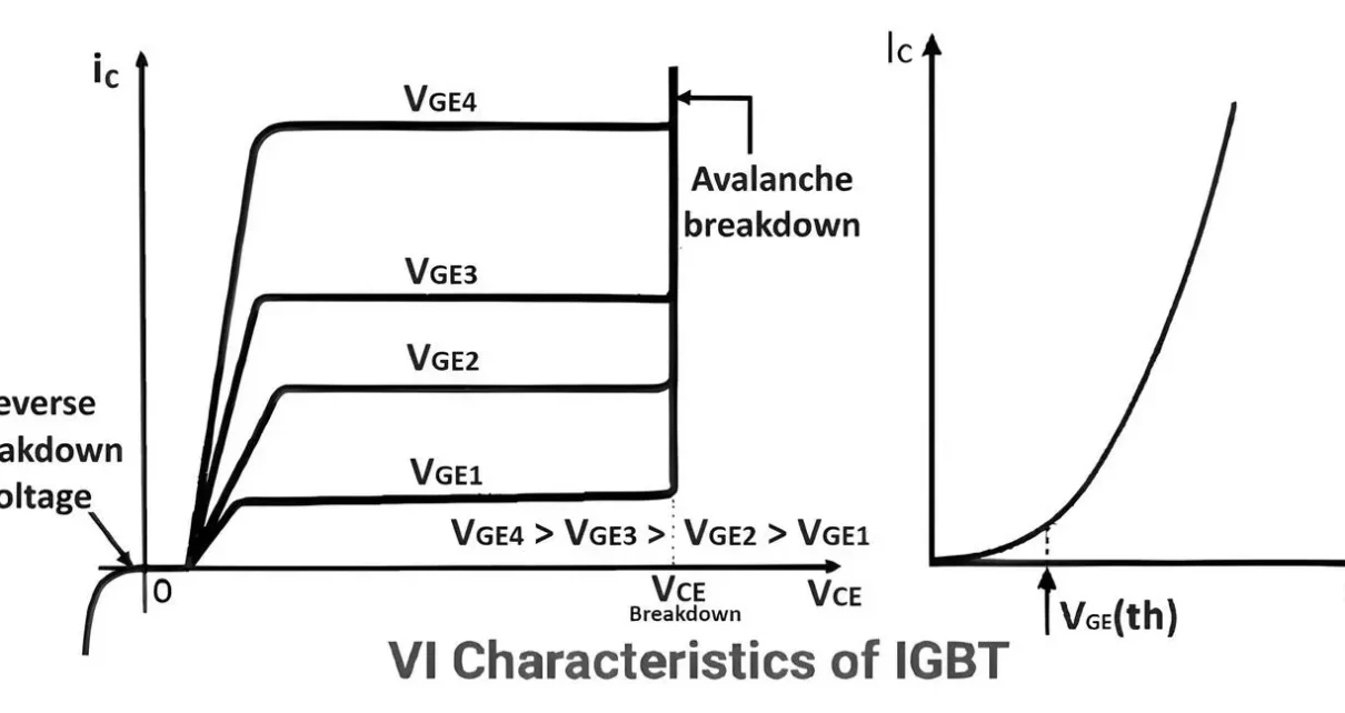
The VI characteristics of IGBT is as shown in Figure. In the forward direction, they are similar to those of bipolar transistors. The only difference here is that the controlling parameter is the gate to source voltage Vgs and the parameter being controlled is the drain current. The working principle of IGBT is based on Conductivity modulation.
An insulated-gate bipolar transistor (IGBT) is a three-terminal semiconductor device it is a hybrid of MOSFET and BJT for high efficiency and fast switching. Read this article to know about the structure of IGBT working and applications of IGBT.
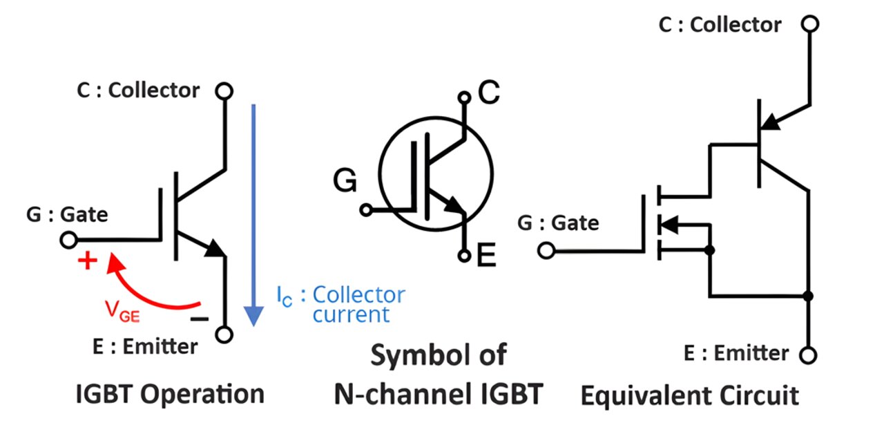
The power BJT has the advantage of low on state power dissipation, but it cannot be switched at faster rates due to longer turn-off time, whereas MOSFETs have a very high switching speed but their power handling capacity is not as good as that of BJTs.
VI characteristics of IGBT:
Thus, IGBT is a voltage-controlled device with an insulated gate. The drain current increases with increase in Vgs at a constant value of Vds
The IGBT possesses all the advantages of MOSFET due to the insulated gate. It also has all the advantages of the BJT due to bipolar conduction.
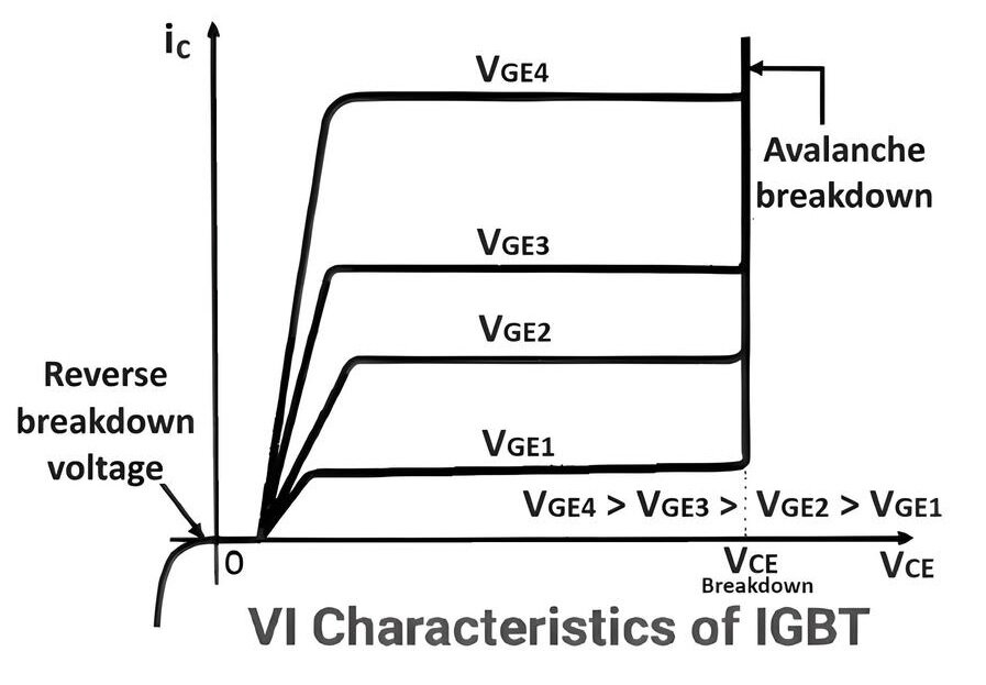
As seen from the VI characteristics of IGBT the drain current (or the collector current) increases with an increase in the voltage between gate and source (Vgs).
Also, note that the gate to source voltage Vgs is positive. Vds is the forward breakdown voltage.
This is the value of Vds at which the avalanche breakdown takes place. At this point the voltage across the device and current through it both are high.
Therefore, the power dissipated in the device will be very large and will damage it. The device must be therefore operated below this voltage.
Transfer Characteristics of IGBT:
The transfer characteristics of an IGBT describe the relationship between the gate-emitter voltage () and the collector current () while keeping the collector-emitter voltage () constant. How IGBT behaves in response to changes in the gate-emitter voltage.
- Threshold Voltage (): This is the minimum gate-emitter voltage at which the IGBT begins to conduct. Below this voltage, the device remains off and the collector current is essentially zero.
- Linear Region: When is just above the threshold voltage, the collector current increases linearly with . In this region, the device behaves similarly to a MOSFET where the current is controlled by the gate voltage.
- Saturation Region: As continues to increase beyond the linear region, the collector current increases more rapidly until it reaches a point where further increases in result in only marginal increases in . This is the saturation region where the IGBT is fully on.
IGBT Transfer Characteristics Curve
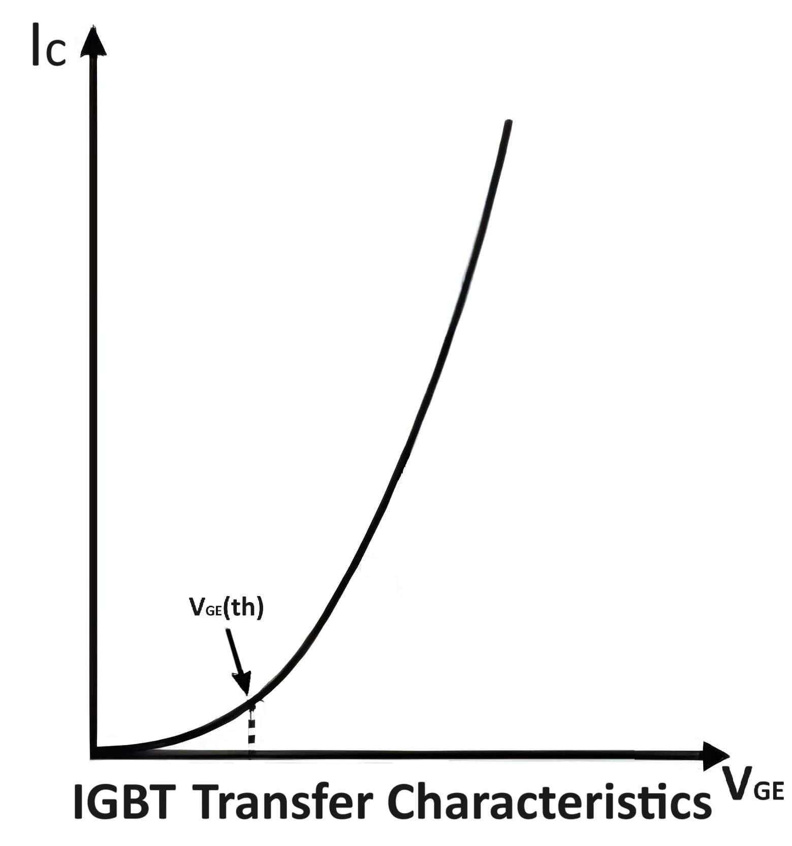
A typical transfer characteristics curve for an IGBT can be plotted with on the vertical axis and on the horizontal axis. Here’s how the curve can be interpreted:
- Off-State (Cutoff Region): For , . The IGBT is off and no significant current flows through the collector.
- Active Region (Linear Region): For slightly above , increases linearly with . The slope of this part of the curve represents the transconductance of the IGBT.
- Saturation Region: For higher values of , the curve flattens out, indicating that is increasing less rapidly with further increases in . The IGBT is fully on in this region, and is primarily determined by the load and .
Mathematical Representation
The relationship in the active region can be approximately represented as:
where is a constant dependent on the specific IGBT.
Practical Considerations
- Gate Drive: To fully turn on an IGBT and operate it in the saturation region, the gate-emitter voltage should be sufficiently higher than the threshold voltage (typically 10-15V for most IGBTs).
- Temperature Dependence: The threshold voltage and transfer characteristics can shift with temperature, generally decreasing with increasing temperature.
- Gate Charge: The dynamic behavior of the IGBT during switching is also influenced by the gate charge, which affects how quickly the gate voltage can be changed.
Types of IGBTs:
Depending on whether the n+ buffer layer has been included in the structure of IGBT or not, they are classified into two categories:
- Non-punch through IGBT (n+ layer is absent). Punch through IGBT (n+ layer present).
- The non-punch through type IGBTs have a symmetrical blocking capacity. That means without breaking down they can block high positive and negative voltages ( Vds) successfully.
- The punch through IGBTs has asymmetrical blocking capacity. That means they can block positive Vds successively but cannot block negative voltage successfully.
Principle of Operation of IGBT:
The principle of operation of IGBT is similar to that of a MOSFET.
The operation can be divided into two parts: Creation of the inversion layer and
- Creation of inversion layer.
- Conductivity modulation.
Creation of inversion layer:
The operation of IGBT is based on the principle of creation of an inversion layer which is the same as that for the power MOSFET.
In IGBTs also when the positive gate to source voltage Vgs is greater than Vgs (threshold), the n-type inversion layer is created beneath the SiO2 (oxide) layer as shown in Figure.
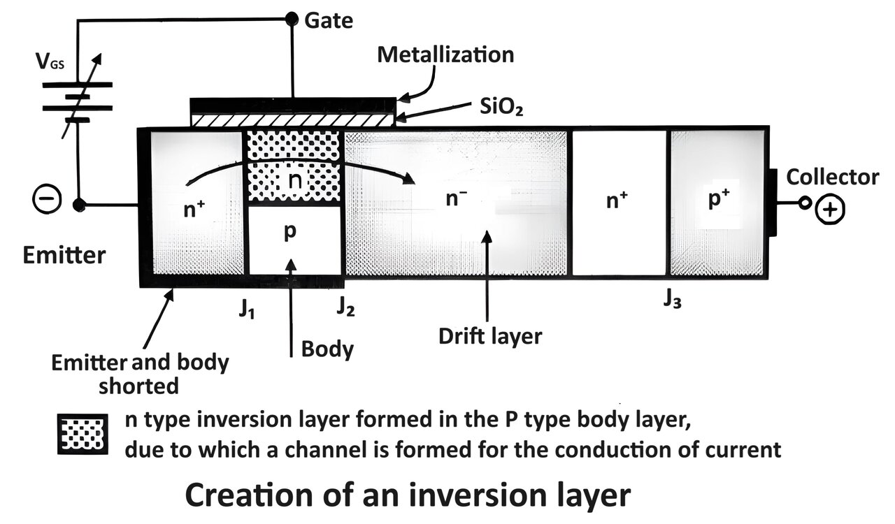
Due to the formation of the n-type induction layer in the p-type body layer, a channel is formed (n+ n n-) which helps to establish the electron current.
The only difference between the MOSFET and IGBT is that there is no “conductivity modulation” of the drift layer in MOSFET.
Therefore, the on-state resistance Rds and hence the on-state power loss is very high in MOSFET. In IGBT however, the conductivity modulation takes place which reduces the on-state loss as explained as follows:
Conductivity modulation:
In IGBT the conductivity modulation of the n- drift layer takes place.
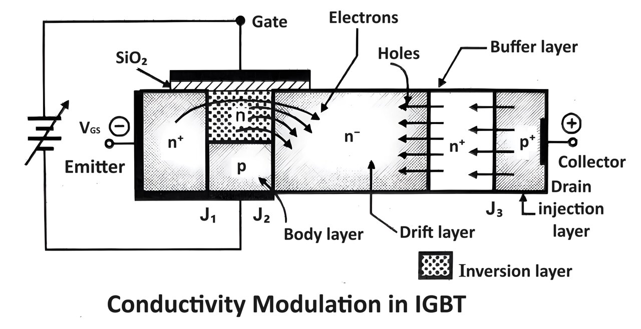
The effect of conductivity modulation is a reduction in the on-state resistance and hence the on-state power loss. Therefore, the on-state losses in IGBT are less than that in MOSFET.
The conductivity modulation in the n- drift layer can be explained with the help of Figure.
Due to the application of a forward voltage between the drain (collector) and source (emitter) the junction J3 is forward biased.
Due to the creation of the inversion layer. electrons from the source are injected into the n- drift layer via the n+ pn- channel.
As the junction J3 is already forward biased, it will inject holes into the n+ buffer layer from the p+ layer.
The electrons injected in the n- drift layer creates a space charge which will attract holes from the n+ buffer layer which were injected by the p+ layer.
In this way “double injection” (of electrons and holes) takes place into the n- drift region from both sides.
This increases the conductivity of the drift region and reduces the resistance to its minimum. In this way, the conductivity modulation will reduce the on-state voltage across the IGBT.
TRIAC Full Form, Symbol, Working, VI Characteristic & Application
Gunn Diode Working Principle VI Characteristics & Applications
