In this article we will be diving into the Aluminum PCB Manufacturing, a type of PCB widely popular in LED light segment for its heat management capabilities. Printed Circuit Boards or PCBs are considered the backbone of electronic devices. The printed circuit board is a miraculous development in the field of technology which is utilized in all types of electronic devices, even simple gadgets such as calculators and digital clocks.
PCB is responsible for directing the current throughout the surface of a device with a complex or simple network of copper paths depending on the application. The designers are being recommended to visit the company from which the PCBs are intended to be fabricated before even designing the original circuit. The step is vital for designers as it prevents them from making any unwanted errors during the design process of PCBs.
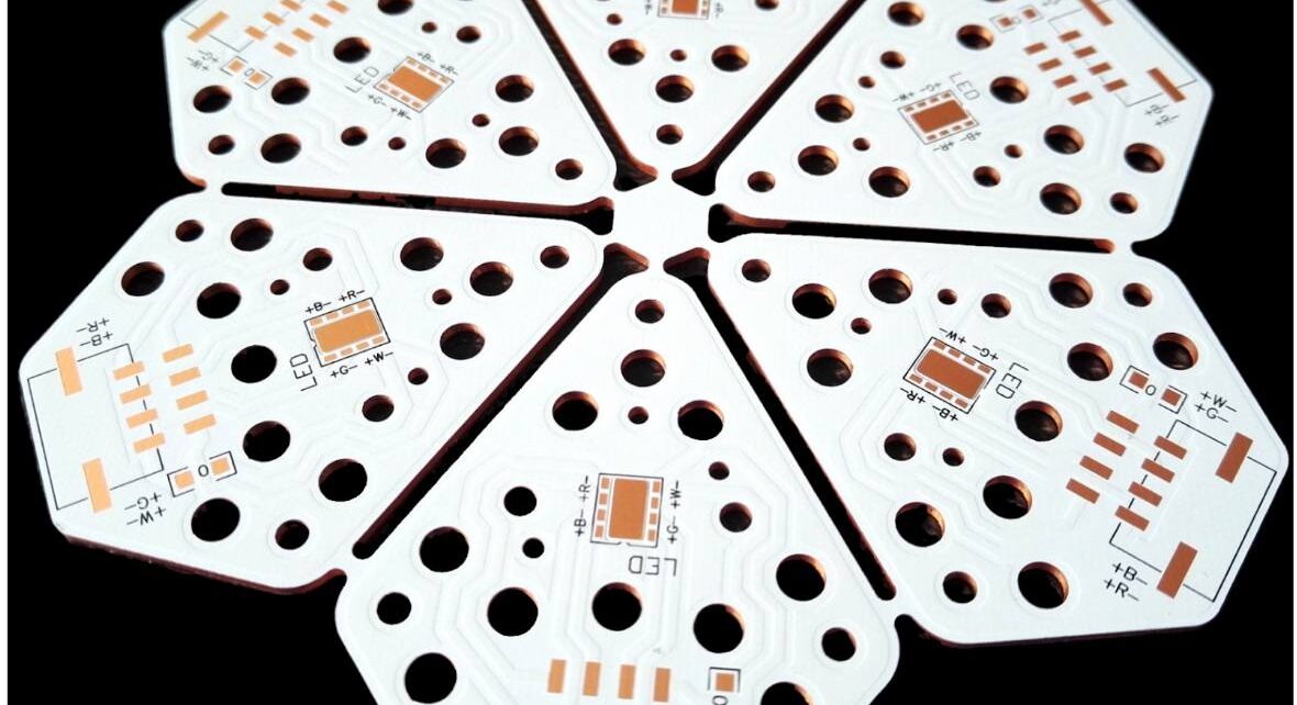
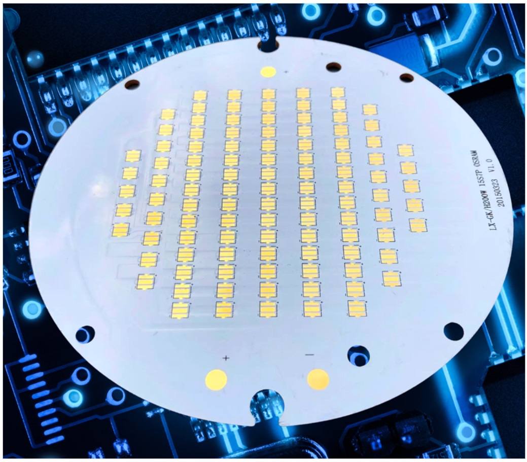
Aluminum PCB is a circuit board produced by aluminum base and dielectric with high thermal conductivity, so we also call it aluminum core PCB. Aluminum circuit boards are always designed as one conductive layer but can also be two layers or multilayers. It is widely used in LED industries, such as traffic lights, indoor house and outdoor lighting, automotive lighting, etc. This article deals with the details of key stages of the manufacturing process of aluminum PCB.
Aluminum PCB Manufacturing Process
The process of fabricating aluminum PCBs is almost the same as for FR-4 printed circuit boards. However, aluminum PCBs require certain dedicated techniques for handling different properties of aluminum, such as profiling is much hard than FR-4 since aluminum material is much more robust then FR-4 material. Following are the main stages that are followed by almost every PCB manufacturer when producing aluminum printed circuit boards.
Designing the Layout
The first and foremost step is designing the layout of the circuit board with the help of software such as EagleCAD or KiCad. Designers must inform manufacturers regarding the software that they are using for designing PCBs to avoid any discrepancies. The next step is translating the design into Gerber files that consist of the images of every layer of the printed circuit board such as copper layers, solder mask, and silkscreen.
The software on which PCB is being designed is performing oversight algorithms to ensure no errors get undetected. During this process, the designers are also examining the PCB design for the width of tracks, spacing of board edges, and size and spacing of holes. After extensive examination of the design and rectification of all possible errors, the designers forward the PCB design and layout for production. Since aluminum PCBs are usually one layer with a big trace width and spacing, an aluminum core PCB layout is not difficult.
Selection of Material
The base material or aluminum circuit board substrate is chosen based on the electrical and thermal properties. The most widely used options consist of aluminum alloys 5052, 6061, and 7075. The thickness of the substrate is usually ranging from 1.0 to 6 millimeters, but the most usually used thickness is 1.6mm.
File to Film
Before printing the design of the PCB, a check is performed known as DFM or design for manufacturability. The DFM check is performed by the manufacturer with the help of a dedicated printer known as a plotter making photo films of the circuit boards for its printing. The manufacturers are utilizing the films for PCB imaging. The result of printing is in the form of a plastic sheet having a negative image of the PCB with black ink. The clear parts on the board are non-conductive material while a black portion represents conductive copper layers. For achieving perfect alignment of the films, hole registration is supposed to be punched within the entire film.
Inner Layers Printing
The film’s creation in the 2nd step was for mapping the figure of the path of copper. This step comprises printing the figures on the copper foil of aluminum substrate. This step is meant for the creation of a PCB pattern. An aluminum printed circuit board is a laminate board consisting of aluminum base and dielectric with a high thermal conductivity as core material known as substrate. This substrate serves as the body of the printed circuit board. The laminated side with copper is cleaned and passed over a decontaminated environment. Afterward, the panel receives a photoresist which is a photo-sensitive layer. This step is only required when the circuit boards are of more than one layer.
Removal of Excess Copper
Excess copper is removed from the board to avoid any technical problems such as short-circuits. For this purpose, a rigorous chemical solution is utilized for the unwanted removal of excess copper. The copper solvent solution removes exposed copper that is unwanted, while copper in desired locations remains protected below the photo-resist layer. All of the copper boards are not created equally but some boards require a huge quantity of copper solvent. However, heavy copper boards require more dedication in tracking the spaces.
Alignment of Layers
When all of the layers are clean enough then alignment is punched to make sure that they work together perfectly. The registration holes are aligning the inner layers with the ones on the outer side. The technician is responsible for placing all layers onto a machine known as optical punch permitting accurate correspondence for accurate punching of registration holes. After the placement of layers is done, it is then impossible to make any changes in the layers on the inner side. An optical inspection is done with an automatic machine for confirmation that no further defects lie in the board. Although aluminum PCBs are always just one to two layers, but we still need to achieve good alignment before lamination.
Lamination
Before lamination, the aluminum substrate’s surface is to be prepared to enable good adhesion of the foil of copper along with some more coatings. This involves degreasing, texturing, and desmutting. Degreasing is achieved with the help of organic agents and oils through the utilization of solvents. Desmutting is the removing layer of aluminum oxide through the utilization of alkaline or acidic agents. Texturing is the creation of microscopic-level roughness over the board surface with mechanical or chemical agents. Certain specific techniques are utilized for the preparation of the surface like acid dipping, chemical etching, and mechanical scrubbing. When the surface is cleaned and treated well, copper sheet and dielectric will be laminated together.
Out Layer Copper Pattern and Etching
Firstly, print the out-layer copper pattern on the copper foil. The layer of copper is coated through a photoresist which is afterwards exposed to ultraviolet radiation with the help of photo tools that are created with printed circuit board design. After the development of the resist, the copper that is exposed is etched completely to create the desired pattern on the circuit board.
Drills and Copper Plating
The next step is drilling holes into the aluminum circuit board so that inner and out layer copper traces can be connected. The drill machine is capable of achieving a diameter of around 100 microns when compared to a hair which is 150 microns. X-ray locator is utilized for the identification of the exact location of the drills for proper targets. A technician places a buffer material board below the target drills to ensure clean drilling of holes. Buffer material prevents the tearing of the board when the drill gets evacuated. Furthermore, the drilled holes’ entire walls are plated electroless to ensure superconductivity. The most commonly used metals for plating are silver, copper, and gold. But for aluminum PCB manufacturing, the drill size and copper width are always bigger compared to FR-4 PCB.
Application of Silkscreen and Solder Mask
The copper-based circuit board is then applied with a layer of solder mask to prevent the solder from bridging among pads while components are mounted onto the board. Different openings are being created through solder masks at various locations that require soldering. Afterwards a layer of silkscreen is printed onto it which identifies the components to be placed and gives information on the polarity of the circuit board.
Routing and Profiling
The bigger printed circuit board panel is routed mechanically for division into smaller units of printed circuit boards that are required. Breakaway tabs are dedicatedly utilized for holding the panels for easy handling. Punching is commonly used in aluminum core PCB production.
Inspection and Testing
Every printed circuit board that is completed is sent for final inspection and testing. Certain electrical and non-electrical parameters are tested such as component fitting, conductivity, and hole plating, etc. Furthermore, automatic optical inspection is performed on the printed circuit boards. Inspection and testing are critical for every printed circuit board, including aluminum PCBs.
Penalization
Before starting the process of assembly, the units of printed circuit boards are arranged in the form of a panel having specific score lines that separate individual boards. This allows the autonomous assembly process for multiple boards over a single panel.
Assembly Process
The entire set of components is soldered over the printed circuit board through a manual or automatic process. Manual assembly is done with bare hands while automatic assembly is either done through surface mount technology or hole-through technology. Aluminum PCB assembly is usually very easy, but needs to be very high speed to save cost.
Electrical Tests
Engineers and technicians perform certain specific electrical tests on the printed circuit boards that are acquired after the assembly process. This automatic process confirms the functionality of the circuit board and confirms the original design. Certain tests are performed such as resistance testing, capacitance testing, continuity testing, comparative testing, flip testing, clamshell testing, and adjacency testing. Functional testing is very suitable for aluminum core PCB production.
Packaging and Shipment
The final step is the packaging of the printed circuit boards that are being manufactured. Packaging is of different types and sizes depending on the kind of PCB either small, medium, or large boxes which are then shipped.
Conclusion
The aluminum printed circuit boards offer numerous benefits for different types of applications in which there are requirements for maintenance of higher power and excellent thermal management. The fabrication procedure of Aluminum PCB manufacturing requires dedicated and state-of-the-art methods such as drilling, plating, profiling, treatments of surfaces along with lamination processes. Aluminum circuit boards are widely used worldwide in lots of industrial area, especially in all kinds of LED products.

Nice article
Please keep writing such nice articles
Good Job!