An OR Gate is one of the most fundamental building blocks in digital electronics. It is a type of logic gate that performs a basic Boolean operation known as logical addition.
In simple terms, an OR gate produces an output when any one or more of its inputs are HIGH (1). The output becomes LOW (0) only when all inputs are LOW.
OR gates play a critical role in enabling decision-making where multiple conditions can trigger an action. They are widely used in digital circuits, microprocessors, alarm systems, control logic, and signal combining applications.
They are essential because complex digital systems are built using combinations of simple logic gates, and the OR gate is one of the core elements used to implement parallel logic conditions.
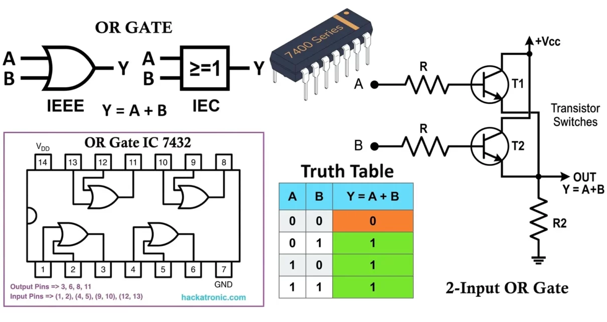
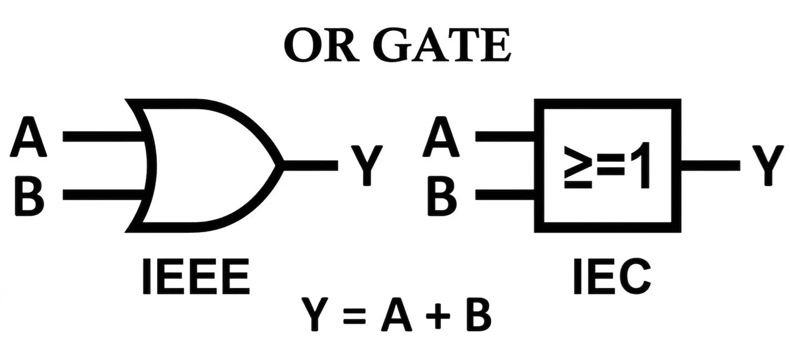
Symbol of OR Gate
- Standard Symbol (ANSI)
- The most commonly used symbol (ANSI standard) consists of:
- A curved input side (concave shape on the left)
- A pointed curved output side (convex shape on the right)
- Two or more input lines entering from the left
- One output line exiting from the right
- The most commonly used symbol (ANSI standard) consists of:
- IEC Symbol
- Represented as a rectangle
- Inside marking: ≥1 (means “one or more inputs HIGH”)
- Inputs enter from the left, output exits from the right
- Multi-Input Symbol
- Additional input lines are added on the left
- The logic remains unchanged: Output is HIGH if any one or more inputs are HIGH
- Terminal and Notation
- Inputs: A, B, C, D…
- Output: Y or Q
- Boolean expression: Y = A + B
- Plus sign ( + ) represents OR operation (logical addition)
- Important Observations
- No inversion bubble → Pure OR operation
- If a bubble is added at the output → becomes a NOR gate
- Output depends on presence of at least one HIGH input, unlike AND which requires all inputs HIGH
OR Gate Truth Table
-
- Working Principle
- The OR gate operates based on a flexible condition:
- Output is HIGH (1) when ANY input is HIGH (1)
- Output is LOW (0) only when ALL inputs are LOW (0)
- The OR gate operates based on a flexible condition:
- Boolean Logic
- The OR operation follows the Boolean addition rule:
Y = A + B
- This is why it is called an addition logic gate.
- The OR operation follows the Boolean addition rule:
- Working Principle
- Key Condition
- ANY input = HIGH → Output = HIGH
- ALL inputs = LOW → Output = LOW
- If A = 1 or B = 1 → Y = 1
- Only if A = 0 and B = 0 → Y = 0
- This makes the OR gate highly useful in trigger-based and parallel condition logic circuits.
- Explanation:
- Row 1: Both inputs LOW → Output LOW
- Row 2: One input HIGH → Output HIGH
- Row 3: One input HIGH → Output HIGH
- Row 4: Both inputs HIGH → Output HIGH
- Key Observation: Output is HIGH if at least one input is HIGH
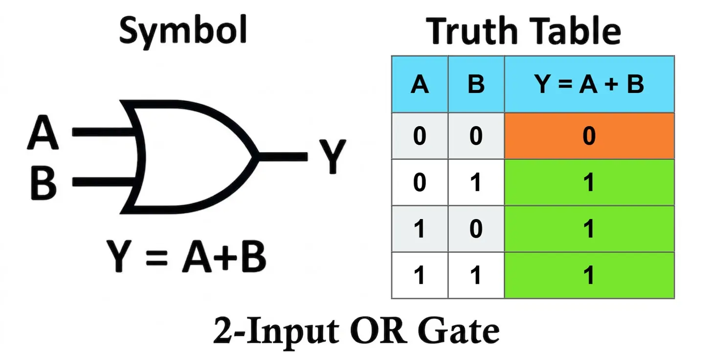
- Extended Form:
Y = A + B + C + D …
- Truth Table Insight
- OR gate acts as a logical “trigger system”
- Even one HIGH input is enough to activate the output
- Widely used in alarm systems, signal detection, and control logic
- Multi-Input OR Gates
- Can have more than 2 inputs
- Used in complex digital systems where multiple conditions can independently trigger an output
OR Logic Circuit Implementation
Diode OR Gate (Diode Logic)
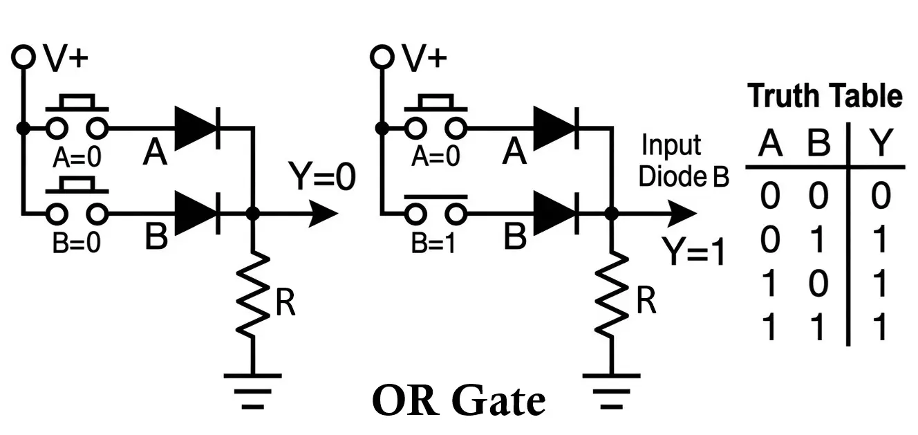
- Components
- Diodes (D1, D2)
- Resistor (pull-down resistor)
- Working
- If any input = HIGH, the corresponding diode becomes forward biased → output becomes HIGH
- If all inputs = LOW, no diode conducts → resistor pulls output LOW
- Key Behavior
- HIGH signal flows through any conducting diode
- Output follows logical OR condition
- Limitation
- Voltage drop across diode (~0.7V for silicon)
- Output is slightly lower than input HIGH
- Not suitable for high-speed or precise logic circuits
Transistor OR Gate (RTL / TTL Concept)
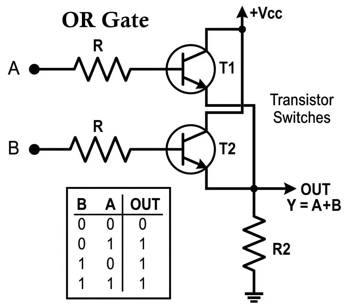
- Working Principle:
- Transistors act as switches
- Connected in parallel configuration
- Operation
- If any input is HIGH → corresponding transistor turns ON → output becomes HIGH
- If all inputs LOW → all transistors OFF → output LOW
- Key Insight
- Parallel configuration ensures OR behavior
- Any conducting path → output activated
CMOS OR Gate
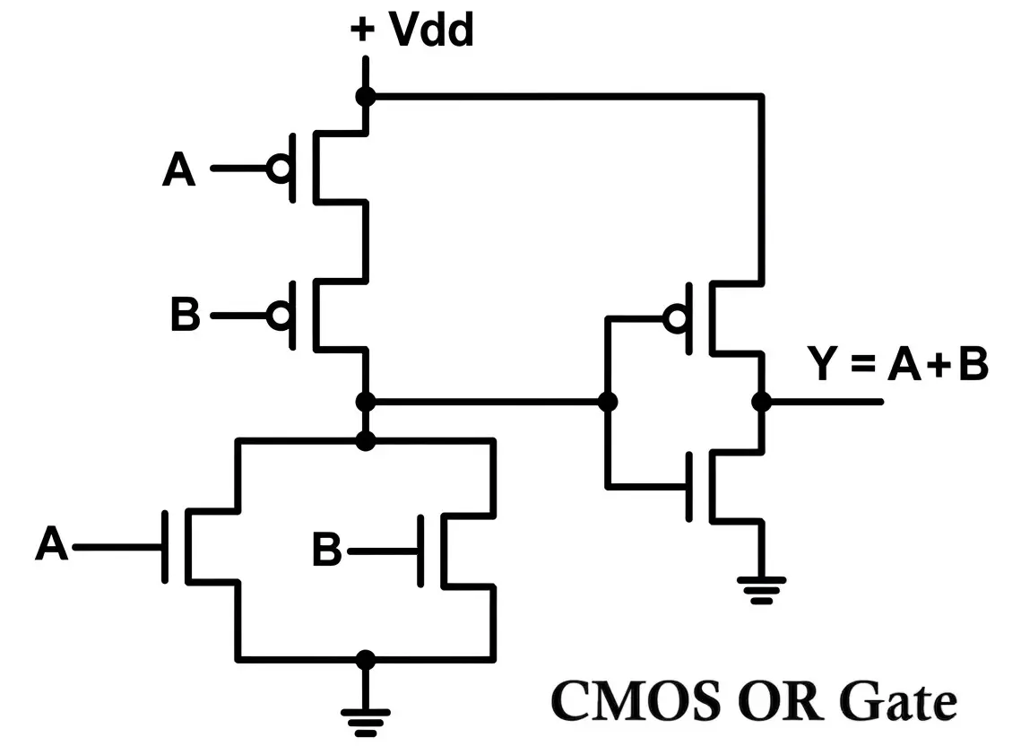
- Structure
- Uses PMOS transistors (pull-up network)
- Uses NMOS transistors (pull-down network)
- Configuration
- PMOS: Series → ensures correct pull-up condition
- NMOS: Parallel → allows output LOW when needed
- Working
- If any input HIGH → NMOS path conducts appropriately and PMOS network adjusts → output HIGH
- If all inputs LOW → PMOS pulls output HIGH? (No, correction: in OR CMOS, output HIGH when input HIGH via logic structure—implementation often derived via NOR + inverter in practice)
- Advantages
- Low power consumption
- High noise immunity
- Dominant in modern VLSI and IC design
NOR Based OR Gate
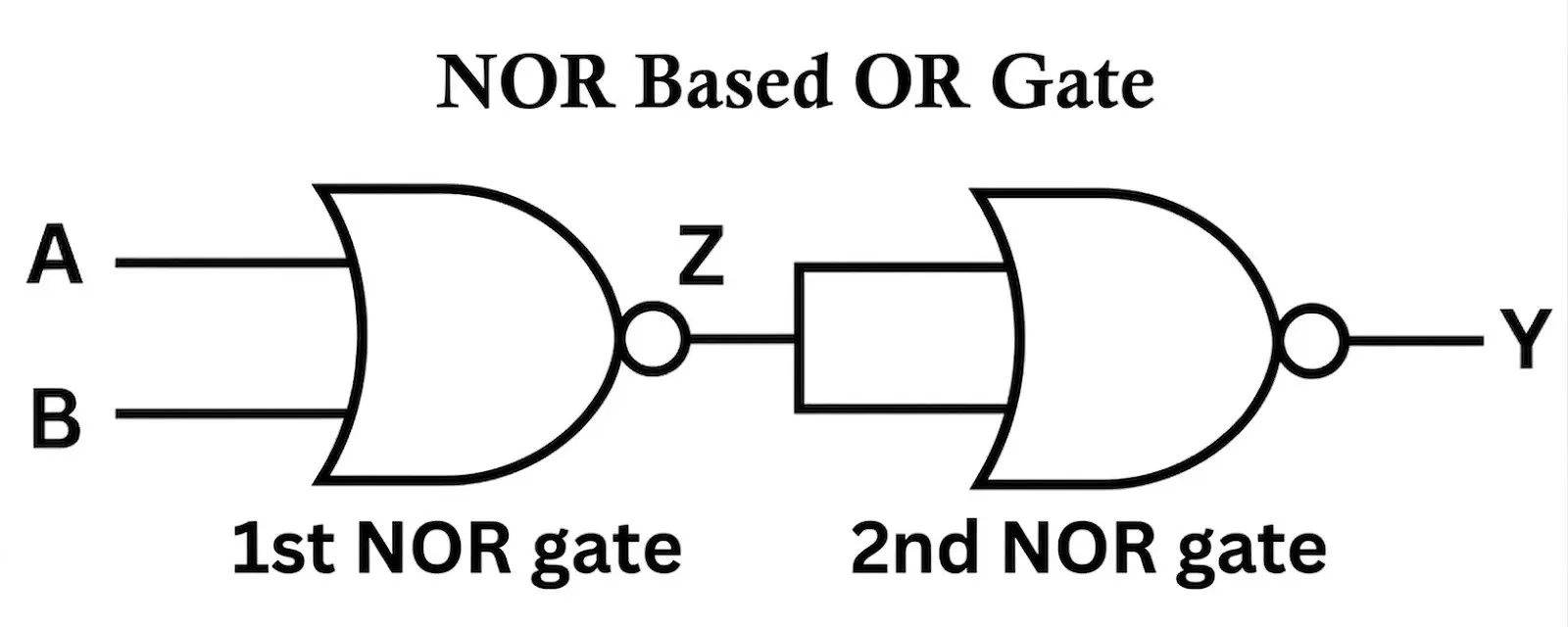
- Boolean Expression:
Y = A + B = NOT(NOT(A + B))
- Implementation
- First NOR gate produces: (A + B)̅
- Second NOR (used as inverter) gives final OR output
- NOR Gate
- NOR = NOT + OR
- Output is inverse of OR: Y = (A + B)̅
- Key Insight
- NOR is a universal gate
- Any logic circuit (including OR) can be implemented using only NOR gates
IC Numbers and Details
OR Gate IC 7432
The 7432 OR Gate IC is a very popular Quad 2-input OR gate integrated circuit belonging to the TTL (Transistor-Transistor Logic) family.
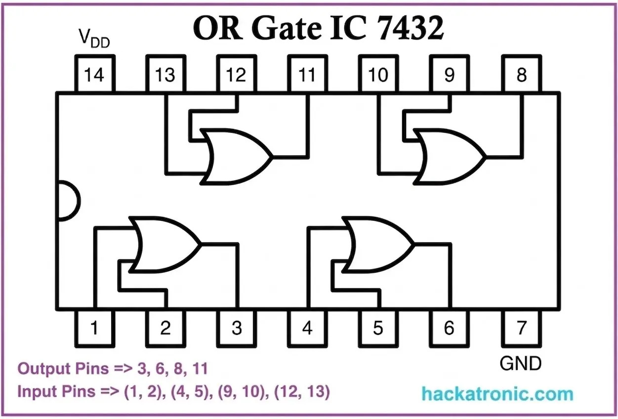
- Features
- Quad 2-input OR gates (4 OR gates inside)
- Technology: TTL (BJT-based)
- Propagation delay: ~10 ns
- Power consumption: ~2 mW per gate
- Supply voltage: 5V (fixed)
- Fan-out: ~10 TTL loads
- Pin Configuration
- Total pins: 14
- 4 OR gates inside the IC:
- Gate 1: Pins 1, 2 → Output 3
- Gate 2: Pins 4, 5 → Output 6
- Gate 3: Pins 9, 10 → Output 8
- Gate 4: Pins 12, 13 → Output 11
- Power Pins:
- Pin 14: Vcc (+5V)
- Pin 7: GND
Key Characteristic: Each gate operates independently, allowing multiple OR operations within a single IC, very useful in compact digital designs.
74LS32 – Low-Power Schottky TTL OR Gate
The 74LS32 belongs to the Low-Power Schottky (LS) TTL family, optimized for better speed and lower power than standard TTL.
- Specifications
- Technology: TTL with Schottky transistors
- Propagation delay: ~10 ns
- Power consumption: Moderate (~2 mW per gate)
- Supply voltage: 5V (fixed)
- Fan-out: ~10 TTL loads
Key Characteristic: Provides a balanced trade-off between speed and power efficiency, making it widely used in traditional TTL systems.
74HC32 – High-Speed CMOS OR Gate
The 74HC32 is part of the High-Speed CMOS (HC) family, combining CMOS efficiency with high performance.
- Specifications
- Technology: CMOS
- Supply voltage: 2V to 6V
- Power consumption: Very low (µW range)
- Propagation delay: ~8–15 ns
- Input impedance: Very high
Key Characteristic: Ideal for low-power digital systems, offering high noise immunity and flexible voltage operation.
74HCT32 – TTL-Compatible CMOS OR Gate
The 74HCT32 is a CMOS device designed to be compatible with TTL logic levels.
- Specifications
- Technology: CMOS with TTL input compatibility
- Supply voltage: Typically 5V
- Power consumption: Very low
- Propagation delay: Similar to HC series
- Input levels:
- LOW ≤ 0.8V
- HIGH ≥ 2V
Key Characteristic: Enables direct interfacing between TTL and CMOS circuits without additional level shifting.
CD4071 – CMOS Quad OR Gate
The CD4071 belongs to the 4000-series CMOS family, optimized for wide voltage operation and ultra-low power consumption.
- Specifications
- Technology: CMOS (4000 series)
- Supply voltage: 3V to 15V
- Power consumption: Extremely low
- Propagation delay: ~60–200 ns (voltage dependent)
- Noise immunity: High
Key Characteristic: Best suited for battery-powered and low-frequency applications, where power efficiency is more important than speed.
IC Comparison Table
| IC Number | Technology | Voltage | Speed | Power |
|---|---|---|---|---|
| 7432 | TTL | 5V | Medium | Medium |
| 74LS32 | TTL (LS) | 5V | High | Low |
| 74HC32 | CMOS | 2–6V | High | Very Low |
| 74HCT32 | CMOS + TTL | 5V | High | Low |
| CD4071 | CMOS | 3–15V | Medium | Very Low |
Timing and Practical Considerations
- Propagation Delay
- Time taken for output to respond to a change in input
- TTL OR gates: ~10 ns
- CMOS OR gates: lower in modern high-speed ICs (HC series)
- Important in high-frequency digital circuits and clocked systems
- Fan-In and Fan-Out
- Fan-In: Number of inputs an OR gate can accept
- Fan-Out: Number of logic inputs the output can drive
- OR gates often have higher fan-in capability in CMOS implementations
- Noise Margin
- CMOS > TTL
- CMOS OR gates provide better immunity to noise and signal disturbances
- Critical for reliable operation in industrial and embedded systems
- Power Consumption
- TTL: Higher power consumption
- CMOS: Very low power consumption (µW range)
- CMOS OR gates are preferred for battery-powered and portable devices
OR Logic Example
- Security System
- Consider a system with two conditions:
- Fire detected (A)
- Gas leak detected (B)
- Output (Y) = Alarm activated
- Alarm is triggered if any one condition is true
- Consider a system with two conditions:
| A | B | Y |
|---|---|---|
| 0 | 0 | 0 |
| 0 | 1 | 1 |
| 1 | 0 | 1 |
| 1 | 1 | 1 |
- Machine Control
- A machine starts when:
- Start button pressed (A)
- Remote signal received (B)
- If any condition is met → Machine starts
- OR logic enables multiple independent triggers
OR Logic Circuit Implementations
- Using Switches (Mechanical Logic)
- Parallel switches represent OR logic
- If any switch is closed → output ON
- Used in basic control panels and wiring logic
- Using Relay Logic
- Relays connected in parallel
- Output activates if any relay is energized
- Common in industrial automation systems
- Using FPGA / Digital Systems
- Implemented using HDL:
assign Y = A | B;
- Used in modern digital design (FPGA, ASIC)
- Implemented using HDL:
Applications
- Logic Simplification
- Boolean algebra simplification
- Karnaugh Maps (K-maps)
- Digital optimization
- In Digital Electronics
- In Computing Systems
- CPU instruction execution
- Logical decision-making
- Memory addressing
- In Everyday Electronics
- Alarm systems
- Industrial automation
- Smart home devices
Advantages
- Simple and easy to implement
- Flexible logic behavior (any input triggers output)
- Reliable operation
- Low cost and widely available
- Works well in parallel decision systems
Limitations
- Cannot perform complex logic alone
- Requires combination with other gates
- May lead to false triggering if inputs are noisy
- Limited functionality in isolation
OR Gate vs AND Gate vs NOT Gate
| Feature | OR Gate | AND Gate | NOT Gate |
|---|---|---|---|
| Boolean Expression | A + B | A · B | A̅ |
| Output Condition | Any input HIGH | All inputs HIGH | Inverts input |
| Output Behavior | Flexible | Strict | Opposite |
Key Differences
- OR Gate: Requires at least one condition to be true
- AND Gate: Requires all conditions to be true
- NOT Gate: Reverses the input logic
Conclusion
The OR gate is a fundamental component in digital electronics that performs logical addition. It outputs HIGH when any input is HIGH, making it essential for trigger-based and parallel decision-making systems.
Key Insights
- OR gate is a flexible logic element
- Used in:
- Alarm triggering systems
- Signal combining
- Control logic
- Multiple symbol standards (ANSI, IEC)
- Truth table defines inclusive logic behavior
- Implemented using:
- Diodes
- Transistors
- CMOS technology
- Available in various IC families:
- 7432, 74LS32, 74HC32, CD4071.
From simple switching circuits to complex processors, OR gates are widely used in systems where any one condition can activate an output. Understanding their working, implementation, and real-world applications is essential for mastering digital electronics.
Types of Logic Gates with Symbol, Truth Table and IC Numbers
Universal NOR Gate Truth Table, Logic Circuit & IC 7402 PIN Diagram
Universal NAND Gate Truth Table, Logic Circuit & IC 7400 Pin Diagram
AND Gate: Symbol, Truth Table, Logic Circuit, and IC Numbers
Classification of Digital Logic Families with Characteristics and Applications
