IC74163 Integrated Presettable Synchronous 4-bit Modulo-16 Up counter. The IC is a synchronous counter as all 4 flip-flops are integrated into the same chip & they receive the same clock pulse (clock signal). The IC74163 is a completely programmable binary counter due to its four preset inputs, which allow it to begin counting with any loaded input by sending a low signal to the load pin. For cascading counters with n-bit synchronous counting, a ripple-carry (RC) output terminal is provided. IC 74163, 74193 74161, etc. are 4-bit binary counters. & IC 7490, 74160, 74190, etc. are the decade counter chips. Find the most basic details about the counter circuit on Decade counter IC7490.
Features of IC74163:
- Typical clock frequency 32MHz
- Typical Power dissipation 93mW
- 4-Bit Modulo-16 Up counter.
- Preset inputs are available
- Synchronously programmable
- Internal look-ahead (Ripple carry) for fast counting
- Carry output for n-bit cascading
- Active low load control line to load input number
- Active low Reset terminal to reset the chip at any point.
- Typical propagation time, clock to Q output 14ns
Block Diagram of IC74163-:
The self-explanatory block diagram of IC74163 is shown in the figure below. If you understand this block diagram, you will be able to design any type of mod-n counter using this IC.
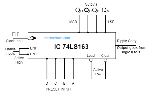
| Pin | Description |
| Clock input | Clock signal input |
| ENP | Enable Parallel(Active High) |
| ENT | Enable Trickle(Active High) |
| Load | Synchronous Parallel Load/Load(Active Low) Input |
| Reset/Clear | Synchronous Active low clear to reset the IC |
| Ripple Carry | Ripple carry is used in cascading |
| A,B,C, & D | Preset Inputs(Parallel Data Inputs) |
| Qn | Flip-Flop Outputs |
What is meant by Synchronous Clear?
Synchronous clear means it is in sync with a clock signal, which means with the next clock signal, the outputs advance to the next count. You need to supply 8 rising clock pulses to reset the IC at a count of 7. You will understand the whole concept once I design the mod 7 counter with 74163.
Functional Description of Pins-:
clock Input
![]()
-:
- It is also known as clock pulse/clock signal, its continuous high-low signal which will use to trigger IC, that’s why it is also known as triggering pulse.
- All 4 flip-flops are triggered with the same clock signal in this IC or any synchronous counter.
Enable Inputs-:
- ENP and ENT are the two enable inputs of the IC74163. Both ENP (Enable Parallel) and ENT (Enable Trickle) should be set to a high value in order to increase the count.
- Both enable pin is active high
- If the clock signal is supplied to IC and low logic is applied to enable terminals the IC will not enable and will not begin counting. for more details refer mode selection table.
Load(Active Low input)-:
- Load this is active low input(logic 0) used to load the data to flip-flop output, If this terminal is supplied with the logic high then the loaded preset input will not be shown in the output.
- If any count is loaded to preset input pins & Low signal(logic 0) is applied to the load terminal then the IC will start counting with the loaded input
- If any count is loaded to preset input pins & high signal(logic 1) is applied to the load terminal, the counting starts with 0000.
Clear (Active Low Input)-:
- This is also known as Master Reset Input, and it’s used to reset the whole IC.
- If this terminal receives an active low signal then it will wait for the next clock signal to reset the output. that’s why it’s known as synchronous clear input.
- Mode Selection Table: (X = Don’t Care for those inputs)
Clear Load ENT ENP Action on the rising clock edge 0 X X X All 4 flip-flop outputs cleared 1 0 X X Load preset inputs data(A, B, C, & D) to Qn 1 1 1 1 Increment Count 1 1 0 X No change (Hold) 1 1 X 0 No change (Hold)
Ripple Carry (R/C logic 0 to 1)-:
- The Ripple Carry terminal (Carry look-ahead circuitry) goes from logic 0 to logic 1, once the IC reaches its maximum count i.e. 1111(15), this signal is used in cascading of IC74163.
- The output of R/C (Ripple Carry) is directly connected to the enable pins of the second IC. As a result, the 2nd IC is only triggered once after each 15th count.
- The 2nd IC gets enabled only once after every 15 counts since the ripple carry goes only once logic 0 to logic 1 after every 15 counts.
Preset Inputs (A, B, C, & D)-:
- A B, C, & D are the preset input, in which A is the Least Significant Bit (LSB) and D is the Most Significant Bit (MSB).
Flip-Flop Output (Qn)-:
- Qa, Qb, Qc, & Qd are the output terminals in which Qa is the Least Significant Bit(LSB) and Qd is the Most Significant Bit(MSB).
Pin Diagram of IC74163-:
The next figure has a self-explanatory pin diagram of IC74163; if you read the figure properly, you will not require to do any more research or briefing on the pinouts.
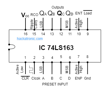
| Pin Number | Description | Pin Number | Description | ||
| 1 | Active Low Clear Input | 9 | Active low Load Input | ||
| 2 | Clock Signal Input | 10 | Active High ENT Input | ||
| 3 | A(LSB) | Preset Inputs to Load Data | 11 | Qd(MSB) | Flip-Flop Outputs |
| 4 | B | 12 | Qc | ||
| 5 | C | 13 | Qb | ||
| 6 | D(MSB) | 14 | Qa(LSB) | ||
| 7 | Active High Input ENP | 15 | RCO(Ripple Carry Output logic 0 to 1) | ||
| 8 | Ground | 16 | Vcc | ||
Mod 7 Counter Using IC 74163-:
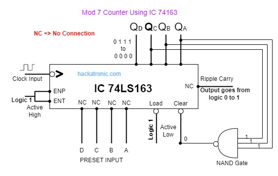
Design Mod 7 Counter using IC 74163? The above counter circuit represents the mod 7 counter using IC 74163 and answers the above question, let’s see how it will work. and how it will automatically start counting from 0000 (0) after reaching 0111 (7).
-
- To start the counting we have applied logic 1 to enable inputs, & load terminals. The output of the NAND gate is connected to the clear pin of IC. the NAND gate will provide logic 1 for the counting states 0000, 0001, 0010, 0011, 0100, 0101, and 0110.
- So, we have received 7 unique states from the above circuit which were motives to design mod 7 counter.
- Once IC receives the next clock signal the count will be incremented to the next state i.e. 0111 and this state will act as input for the connected 3-input NAND gate. The clear terminal will receive logic 0 and reset the whole IC on receiving the next clock signal. since the 74163 is a synchronous counter therefore it is waiting for the next clock signal otherwise it will automatically reset the IC once the clear pin receives logic 0.
- In the manual clocking system, you will see the state 0111, but in the case of the system-generated clocking system, you won’t be able to see the state 0111 as the clocking speed is too fast.
- So you might be confused while providing manual clocks to IC by observing 8 unique states, requesting you please reset the IC at 0110 in manual clocking.
- If want to reset the IC at 0110 then use only a 2-input NAND gate and connect Qb, and Qc, as an input terminal for the NAND gate. then you will get all the 7 unique states and on state 0110 it will wait for the next clock signal to reset the IC.
Happy Learning………….. While opening in the phone select desktop mode as tables are not properly visible due to display size……… please comment for the next article……..

Thank you very much for including the MSB and LSB designations in your diagrams, with “A” being the LSB and “D” being the MSB. That information is not included in the datasheets for the 74LS161/3 Series when it absolutely should be. (Just wish I had run into this page before I laid out my board. I looked all over and could not find a statement of this convention). The letter convention apparently comes from Flip Flop cascades typically being named with letters, starting with “A” and positioned at the far left with the cascade proceeding to the right. This, however, is backwards from the numeric system with MSB on the left, and as such is counter-intuitive. When an arbitrary standard that is in fact counter-intuitive remains unstated throughout all standard technical documents, that is FUBAR territory. Thanks again for unFUBARING this decades long FUBARISH gaff by On-Semi, Texas Instruments, etc… .