A PCB (Printed Circuit Board) is the “skeleton” of an electronic device, while electronic components like resistors, capacitors, chips, and diodes are its “flesh and blood.” Only through a standardized installation process can these components be securely fixed and connected on the PCB to create a complete circuit. Whether it’s a simple toy circuit board or a complex smartphone motherboard or industrial control module, the installation process may vary, but the core logic remains the same: matching the package → precise positioning → securing the connection → testing and verification.
Many people are curious about how these tiny components are “precisely placed” on the PCB. What’s the difference between manual installation and factory automation? How do components with different packages (like DIP or SMD) get installed? This article will break down the entire installation process step by step, starting with component package types, detailing key steps, tools, and important considerations, so you can thoroughly understand how electronic components “connect” with PCBs.
Matching Components with the PCB
Package Matching:
The package of electronic components (such as DIP or SMD) determines its installation method and the design of the corresponding pads on the PCB. Simply put, the pads (metal contact points) on the PCB are designed to match the component package. Only when the component package matches the size and spacing of the pads can it be precisely installed and reliably connected.
Common package types and matching requirements:
- DIP Package (Dual Inline Package): For components like DIP-8 chips and through-hole resistors with long metal pins. The PCB needs to have corresponding “pin holes.” The pin diameter and hole size need to match (usually the pin diameter is 0.1~0.2mm smaller than the hole) to ensure smooth insertion and tight contact.
- SMD Package (Surface Mount Device): For components like 0402 and 0201 capacitors, 3528 and 5050 LEDs, and QFP and BGA chips. These components have no long leads, and the PCB needs to have corresponding “surface-mount pads.” The pad size and spacing should perfectly match the component’s lead or solder pad. For example, the pad length for a 0402 capacitor is about 0.4mm, and the width is about 0.2mm. Ensure that pads are not too large (causing shorts) or too small (causing poor contact).
Polarity Matching:
Some electronic components have polarity (positive and negative terminals). When installing these, they must be matched with the polarity markings on the PCB, or else the component may be damaged, the circuit may short, or the device may fail. Components that require polarity matching include:
- Diodes and LEDs: The longer leg is positive, and the shorter leg is negative. The PCB usually has “+” and “-” marks, or a notch or color ring to indicate polarity.
- Electrolytic Capacitors: The longer leg is positive, and the shorter leg is negative. The capacitor body often has a black ring to indicate the negative terminal, which matches the corresponding PCB marking.
- Chips (like ICs or BGAs): These usually have a positioning mark (such as a notch or dot), and the PCB pad will also have a corresponding mark to ensure the pins align correctly and prevent pin misalignment that could cause shorts.
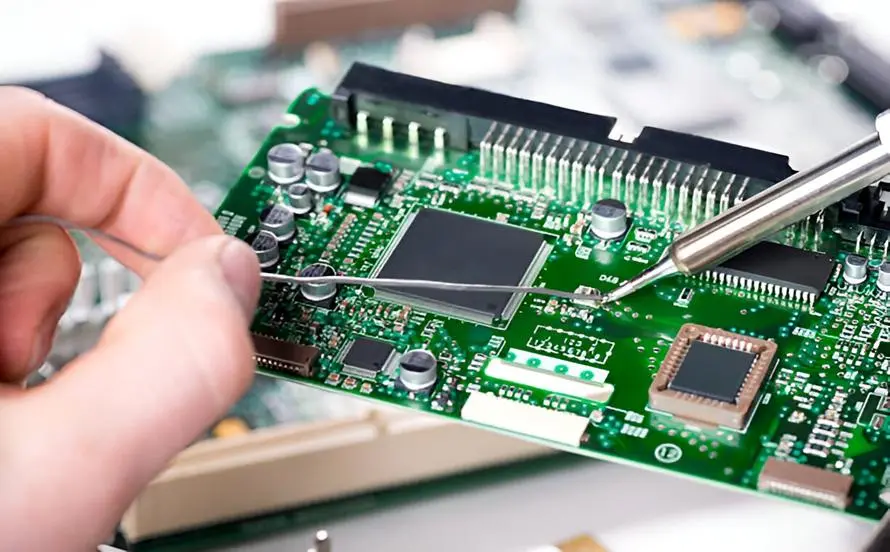
Manual Installation
Manual installation doesn’t require complex equipment. The core tools are a soldering iron, solder wire, tweezers, magnifying glass, and so on. The process is divided into “through-hole installation” and “surface-mount installation” to adapt to different component packages.
Installation Process for Through-Hole Components (DIP Package)
Through-hole components have leads, making manual installation relatively simple. The core steps are: “Insert → Solder → Trim the leads.” Let’s take through-hole resistors or diodes as examples:
Step 1: Preparing the Leads
Gently bend the component leads to match the angle of the PCB holes (usually 90°). This ensures the leads can smoothly go into the holes and avoids breakage from excessive bending.
Step 2: Insertion
Using tweezers, hold the component and align the leads with the corresponding holes on the PCB. Gently insert the leads, ensuring the component body sits flush against the PCB surface (without floating) and the leads come through the PCB’s backside.
Step 3: Soldering and Fixing
Preheat the soldering iron to 350-400°C. First, apply the soldering iron tip to the PCB’s back-side pads for 1-2 seconds to heat them. Then, touch the solder wire to the junction of the pad and lead. Once the solder melts and evenly covers the pad, remove the solder wire first, followed by the soldering iron. Keep the soldering time under 3 seconds to avoid overheating the components.
Step 4: Lead Trimming
Use side cutters to trim the excess lead on the PCB’s backside, leaving about 1-2mm of lead. This prevents overly long leads that could cause shorts and too-short leads that may cause solder joint failure.
Installation Process for Surface-Mount Components (SMD Package)
Surface-mount components are small and lack long leads, requiring higher precision for manual installation. A magnifying glass is often needed. The core steps are: “Positioning → Fixing → Soldering.” Let’s use 0402 capacitors or surface-mount resistors as examples:
Step 1: Aligning the Component
Using tweezers, hold the surface-mount component and, with the help of a magnifying glass, precisely align the component’s leads or solder pads with the corresponding pads on the PCB. Ensure the component is centered and there is no offset (offset can lead to poor soldering).
Step 2: Temporary Fixing
You can apply a small amount of solder to one pad or use flux to temporarily hold the component in place. This ensures the component won’t shift during the rest of the soldering process.
Step 3: Full Soldering
Using the soldering iron, sequentially solder each lead or solder pad. Maintain the soldering iron temperature between 320-380°C to avoid overheating, and ensure the solder covers the pad evenly. Be cautious not to create shorts (when adjacent pads connect) or cold solder joints (when the solder doesn’t fully cover the lead).
Manual Installation Tips:
- Soldering Iron Temperature: Don’t set the temperature too high, as it can burn the components and the PCB, especially for SMD components, which are more sensitive to high temperatures.
- Use Flux: Flux helps the solder flow better and prevents oxidation, improving solder joint quality.
- Check Polarity: Always double-check the polarity of components to avoid incorrect installation.
- Inspect the Joints: After soldering, inspect the joints for cold solder, weak connections, or shorts, and ensure components are not floating or displaced.
Automated Installation
In large-scale manufacturing of electronic products like smartphones, computers, and TVs, manual installation is inefficient and cannot meet the demands of high-density, fine-pitch components. Therefore, “SMT Assembly” are used. The core process involves: “Solder Paste Printing → Component Placement → Reflow Soldering → Inspection” with the entire process being fully automated by equipment, offering higher precision and efficiency compared to manual methods.
Step 1: Solder Paste Printing (Critical Step)
Solder paste is the “bridge” that connects the components to the PCB. It consists of solder powder and flux, and it is in paste form at room temperature but melts at high temperatures to form solder joints. The core equipment for this step is the “screen printer,” and the process is as follows:
- The PCB is securely placed on the screen printer’s workbench, ensuring precise positioning.
- A stencil (corresponding to the PCB pad design with cutout patterns) is placed on top of the PCB.
- The printer’s squeegee spreads the solder paste evenly over the stencil, and the paste passes through the cutouts, accurately printing on the PCB pads.
- After printing, the PCB is removed and inspected for solder paste quality: the paste should be evenly distributed (usually 0.1-0.2mm thick), with no smudging, missing areas, or bridging.
Step 2: Component Placement (Precise Positioning)
This step is performed by a “pick-and-place machine,” which acts like an automated tweezer. It can accurately pick up components and place them on the PCB at designated positions. The process goes as follows:
- Component Feeding: Components are placed into feeders (such as tape feeders or tray feeders), which are connected to the pick-and-place machine. These feeders automatically supply components to the machine.
- Visual Positioning: The pick-and-place machine uses a high-definition camera to detect the PCB’s positioning markers and pad locations, as well as the component’s package and polarity. It then calculates the precise placement coordinates.
- Grabbing and Placing: The machine’s nozzle adjusts its suction strength based on the component size, picks up the component, and moves it to the correct pad on the PCB. The component is placed with even pressure to ensure accurate alignment between the leads/pads and avoid damaging the component or PCB.
Step 3: Reflow Soldering (Securing the Connection)
After the components are placed, they are temporarily held in position by the solder paste. However, the solder paste needs to be melted and fully solidified to form strong, reliable solder joints. This is done through the Reflow Soldering Furnace. Here’s how the process works:
The PCB with placed components is placed on a conveyor belt that moves it through four temperature zones inside the reflow soldering furnace:
- Preheating Zone: The temperature gradually rises (from room temperature to around 150-180°C). This step removes moisture from the solder paste and evaporates flux, avoiding defects like voids during the soldering process.
- Ramp-Up Zone: The temperature rapidly increases to around 200-220°C. This step fully evaporates the flux, cleans the pads and leads of the components, and removes any oxidation.
- Reflow Zone: The temperature reaches the peak (240-260°C, depending on the solder paste type). The solder paste melts, wets the pads and leads, and forms a metallurgical bond between the component leads and PCB pads.
- Cooling Zone: The temperature rapidly decreases, solidifying the solder and fixing the components securely to the PCB.
Step 4: Inspection and Rework (Ensuring Quality)
Once the automated installation process is complete, it’s important to verify the quality. Several types of inspection are performed:
- AOI Inspection (Automated Optical Inspection): A high-definition camera scans the PCB to detect defects like component misplacement, missing components, flipped components, bridging, and cold solder joints. Faulty products are flagged for rework.
- X-Ray Inspection: This is used for inspecting components like BGAs or CSPs, where the pins are located at the bottom of the chip. X-rays pass through the PCB and help detect internal defects like voids or cold solder joints in the hidden areas of the solder.
- Rework: For products identified as defective during inspection, rework is performed. This could involve manually repositioning components, resoldering, or cleaning up bridges. The goal is to ensure that every PCB meets the required quality standards.
Special Component Installation Considerations
Apart from regular components like resistors, capacitors, and chips, there are certain special components that require extra attention during installation. Improper handling of these can lead to component damage or circuit failure. Focus on the following 3 types:
High-Power Components (e.g., Power Transistors, Transformers)
These components generate a lot of heat and are often heavier. Proper installation is crucial:
- Heat Sinks: These components need to be attached to heat sinks to dissipate heat efficiently. The components should be connected to the heat sinks using thermal paste for better thermal conductivity.
- Longer Preheating Time: Since these components are sensitive to heat, preheating time should be extended to prevent damage from concentrated heat.
- Mechanical Stability: Some high-power components require additional mechanical support, such as using screws to fix them to the PCB or external casing, ensuring they stay securely in place.
Sensitive Components (e.g., MOSFETs, Sensors)
These components are sensitive to static electricity and high temperatures. Careful handling is required:
- Static Protection: Operators must wear anti-static wristbands and gloves to avoid electrostatic discharge (ESD) that could damage the components.
- Lower Soldering Temperature: Soldering temperatures should be reduced by 20-30°C compared to regular components to prevent thermal stress.
- Avoid Direct Contact: Avoid touching the sensitive pins of these components to prevent damage.
Irregularly Shaped Components (e.g., Connectors, Buttons, Modules)
These components have irregular shapes, requiring special attention during installation:
- Position First: These components should be positioned and fixed before soldering to prevent misalignment.
- Connectors: For components like connectors that involve plug-and-play operations, ensure strong solder joints to avoid lead breakage during insertion or removal.
- Mechanical Fit: Buttons, LED modules, and similar components must be placed tightly on the PCB surface to ensure proper mechanical contact and stable performance.
How to Judge Installation Quality
Whether manual or automated, evaluating the quality of the component installation is crucial. Here are the three main standards to ensure reliable circuit operation:
- Precise Positioning: Components should not be misaligned or floating, and leads/solder pads must align perfectly. Polarity should also be correct.
- Solder Joint Quality: The solder joints should be full, smooth, and free from voids. The solder should uniformly cover both the pad and lead, with no cold solder joints, poor connections, bridging, or missed joints.
- Mechanical Stability: Components should be firmly fixed without any looseness or movement. High-power and irregularly shaped components should not wobble, and thermal and anti-static measures should be in place.
Conclusion
The process of installing electronic components onto a PCB may seem simple, but it’s really all about the details, from matching component packages, verifying polarity, to precise positioning, soldering, and testing. Every step needs to be executed correctly to ensure a reliable connection between the components and the PCB, which results in a functional circuit.
In fact, many hobbyists and manufacturers now outsource the component installation process to third-party companies that offer PCB assembly services. These services can deliver components at a lower cost, faster speed, and with higher quality, allowing you to focus on design and sales while enjoying the convenience.
Whether you choose to install components manually or through automated processes, understanding the installation process and quality standards is essential for creating reliable electronic products. With the right tools, techniques, and attention to detail, you can ensure that your PCB assembly is successful and your devices perform as expected.
Surface Mount (SMT) vs Through Hole (THT) PCB Assembly Technology
High Speed PCB Design: Essential Wiring Techniques for Optimal Performance
Gold Finger PCB Assembly: Best Practices for Ensuring Reliability
