Let’s explore D flip flop truth table with circuit diagram and working. Also, we will see application of D flip flop in electronic circuit. A D flip-flop, also known as a data or delay flip-flop, is a fundamental building block in digital electronics. commonly used for data storage, synchronization, and control applications. It stores one bit of data (either 0 or 1) and has two stable states, typically referred to as the “set” state (Q = 1) and the “reset” state (Q = 0).
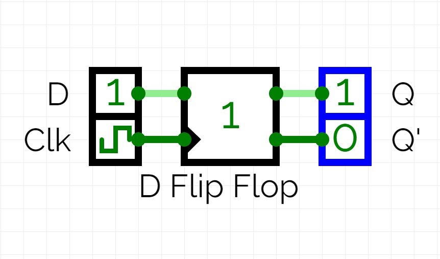
D Flip Flop Circuit Diagram:
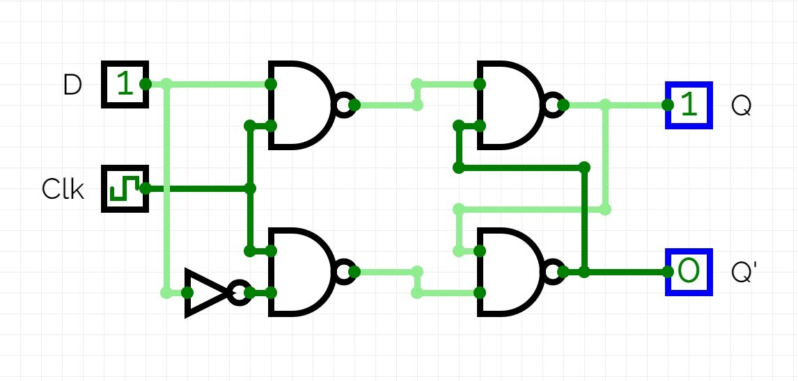
A D flip-flop, also known as a data or delay flip-flop, is a fundamental building block in digital electronics. It stores one bit of data. Here’s a basic circuit diagram of a D flip-flop using NAND gates:
- D is the data input.
- CLK is the clock input.
- Q is the output.
D Flip Flop circuit working:
D flip-flop can be toggled between its two states based on a clock signal. Let’s break down its working:
Inputs: The D flip-flop has two main inputs:
D (Data Input): This is the input that determines the value to be stored in the flip-flop.
CLK (Clock Input): This input is used to control when the flip-flop reads the value on the D input.
Output: The flip-flop has one output:
Q (Output): This is the output that stores the value of the D input. It reflects the value of the D input at the moment the clock signal transitions from low to high (rising edge).
The Working of the Flip Flop is as follows:
- When the clock signal (CLK) transitions from low to high, the input data (D) is transferred to the output (Q). If D is high (1), then Q will be high when the clock signal transitions.
- When the clock signal is low, the output remains in its previous state, regardless of any changes in the input data. If D is low (0), then Q will be low regardless of the clock signal.
| D | CLK | Q(t) | Q(t+1) |
|---|---|---|---|
| 0 | ↑ | Q | 0 |
| 1 | ↑ | Q | 1 |
When the CLK input transitions from low to high (rising edge), the value present on the D input is transferred to the Q output.
The actual implementation of a D flip-flop can vary depending on the technology and specific requirements, but the basic principle remains the same. You can also construct a D flip-flop using NAND and NOR gates, or by using dedicated flip-flop ICs.
D Latch vs D Flip-Flop:
A D flip-flop is edge-triggered, meaning it only updates its output on a specific edge of the clock signal (in this case, the rising edge). This makes it more suitable for synchronous systems where data changes need to be synchronized with the clock. Master slave D flip flop is edge-triggered.
In contrast, a D latch is level-sensitive, meaning it continuously updates its output based on the current values of its inputs, regardless of the clock signal. This makes it more suitable for asynchronous systems where immediate updates are required. The single D flip flop is a latch.
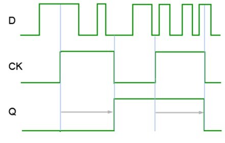
Timing Diagram:
A timing diagram illustrates the behavior of a D flip-flop over time, showing the relationship between the clock signal, the data input, and the output.
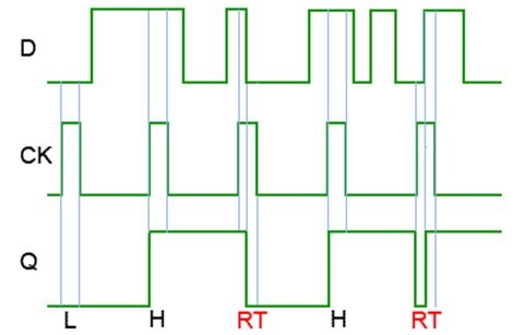
Ripple Through (RT):
“Ripple through” refers to the phenomenon where changes in the input D that occur while the clock signal is high, or transitioning may not immediately affect the output Q. Instead, these changes may propagate through the flip-flop with some delay, potentially causing a ripple effect in subsequent stages of a circuit.
In simpler terms, “ripple through” means that changes in the input might not instantly show up in the output when the clock changes. Instead, there could be a delay, causing a ripple effect through the circuit.
This delay happens because of how the flip-flop works internally. It’s important to consider these delays when designing circuits to avoid timing problems. These issues can be avoided by using Master slave configuration of D flip flop.
Overall, the D flip-flop is a crucial component in digital circuits for its ability to store data based on a clock signal, making it essential for sequential logic and digital communication systems.
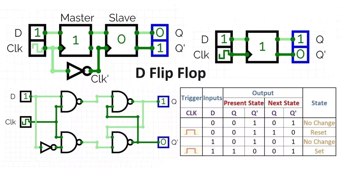
D Flip Flop Master Slave Configuration:
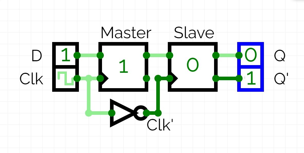
Here’s how it works:
Master latch: On the rising (or falling) edge of the clock signal, the master latch captures the input data (D input). However, it doesn’t immediately propagate this data to the output.
Slave latch: On the opposite edge of the clock signal, the slave latch takes the output of the master latch and stores it. This ensures that the output remains stable between clock transitions and prevents potential glitches.
By using this master-slave configuration, the D flip-flop becomes edge-triggered.
Truth Table of D Flip Flop:
A D flip-flop, also known as a data or delay flip-flop, is a type of sequential logic circuit. It has one data input (D), one clock input (CLK), and two outputs: Q and Q’. The Q output represents the current state of the flip-flop, and Q’ represents its complement.
Here’s the truth table for a D flip-flop:
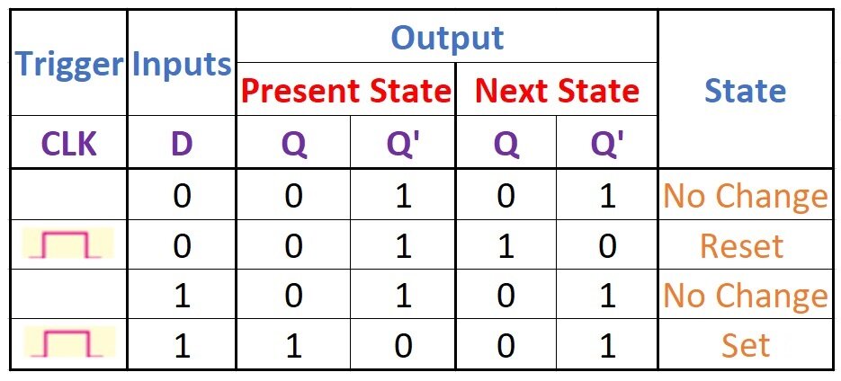
In this truth table:
- D is the input data.
- CLK is the clock signal.
- If Q is the current state of the flip-flop, then Q+1 is the next state of the flip-flop after the clock edge.
The behavior of a D flip-flop is such that the output (Q) changes to match the input (D) only when the clock signal transitions from low to high (a rising edge). When the clock signal is low (0), the flip-flop holds its current state. This characteristic makes it useful for capturing data at specific points in time, which is essential in sequential logic circuits.
D Flip Flop Applications:
Registers:
D flip-flops are often used as the basic storage elements in shift registers and other types of registers. Shift registers are used for serial-to-parallel and parallel-to-serial data conversion, data storage, and various other applications in digital systems.
Counters:
D flip-flops can be connected together to create binary counters. By connecting the output of one flip-flop to the input of another, you can create synchronous binary counters that count in binary sequence.
Frequency Division:
D flip-flops are also commonly used in frequency dividers. By toggling the input of a D flip-flop at a certain frequency, you can obtain a divided frequency at the output, which is useful in clock signal generation and timing applications.
Memory Elements:
D flip-flops are the basic building blocks of memory elements like registers, latches, and memory cells in digital systems. They are used to store binary information temporarily or permanently in various types of memory structures.
State Machines:
D flip-flops are used in the implementation of state machines and sequential logic circuits. State machines are used to control the behavior of digital systems based on their current state and inputs, and D flip-flops play a crucial role in storing the state information.
Data Synchronization:
D flip-flops are often used for synchronizing data in digital systems. By latching data with a clock signal using D flip-flops, you can ensure that the data is sampled at the correct time and avoid issues such as metastability.
Digital Signal Processing:
In digital signal processing applications, D flip-flops are used for storing intermediate results, buffering data, and implementing various processing algorithms such as finite impulse response (FIR) filters and digital oscillators.
Control Logic:
D flip-flops are used in control logic circuits for storing control signals, flags, and status information in microprocessors, microcontrollers, and other digital systems.
These are just a few examples of the many applications of D flip-flops in digital electronics. They are versatile components that play a crucial role in the design and implementation of digital systems and circuits.
JK Flip Flop Truth Table, Circuit Diagram, Working & Applications
