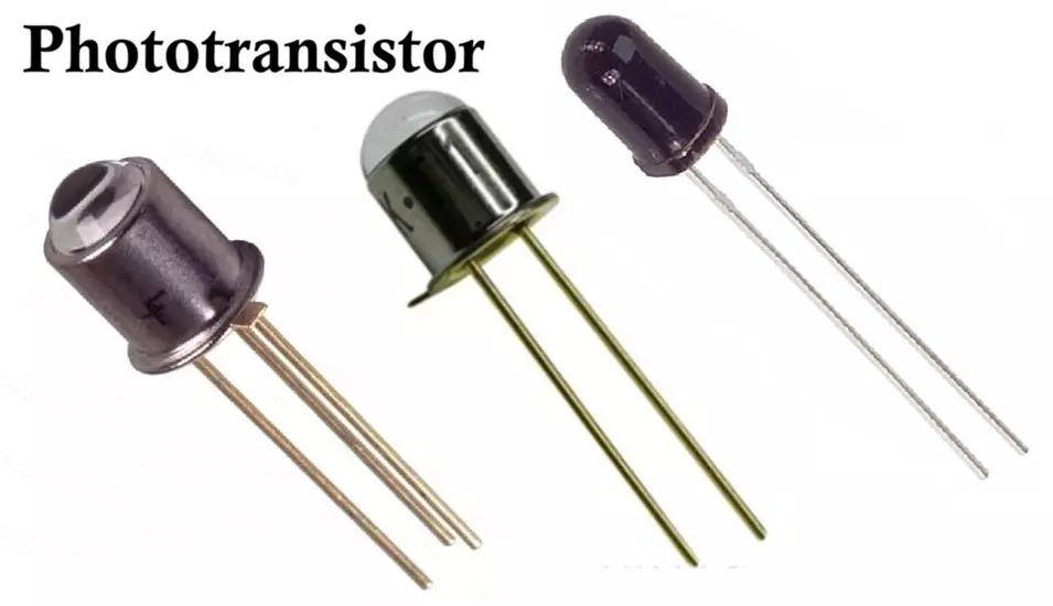
A phototransistor is a semiconductor device that combines the properties of a photodiode and a transistor. It is sensitive to light and provides amplified electrical output based on the light intensity incident on its base region. Phototransistors play a vital role in optoelectronic applications such as light sensing, encoders, switches, and signal transmission, owing to their high sensitivity and fast response.
What is a Phototransistor?
A phototransistor is a semiconductor device that behaves like a switch but is controlled by light instead of electrical current at its base. It essentially acts as a light-sensitive switch or amplifier – when light falls on its photosensitive surface, it generates base current, allowing a much larger current to flow between the collector and emitter.
- A phototransistor converts light energy into electrical signal.
- Provides amplification — it’s more sensitive than a photodiode.
- Used in light detection, optocouplers, optical switches, light meters, etc.
Thus, the phototransistor switches or amplifies the output signal in proportion to the light intensity.
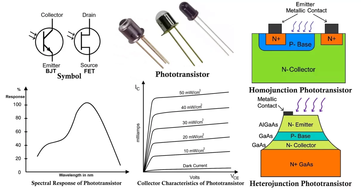
Symbol of a Phototransistor
The symbol looks like a regular BJT transistor but with arrows pointing toward the base region to indicate incoming light.
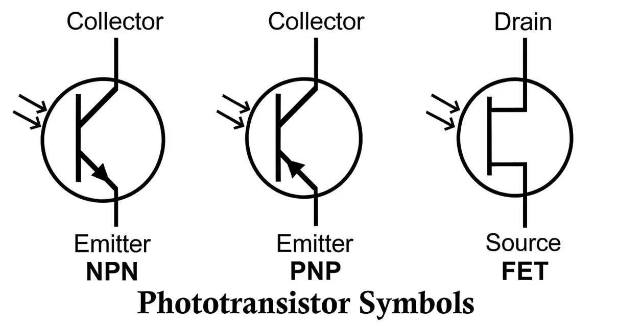
- Arrows (→) point toward the base region, representing light hitting the phototransistor.
- Collector (C) at the top.
- Emitter (E) at the bottom.
- The base is usually not brought out as a physical pin.
Terminals of a Phototransistor
A phototransistor typically has 2 or 3 terminals:
- Collector (C) — usually positive in NPN-type phototransistors.
- Emitter (E) — usually grounded or connected to the negative terminal.
- Base (B) — often no base pin is present, light acts as the base input. (In some types, a base pin is brought out for optional biasing.)
- 2-terminal phototransistor: just collector and emitter, with light as input.
- 3-terminal phototransistor: collector, emitter, and a base pin for additional control.
Construction of Phototransistor
A phototransistor is essentially a bipolar junction transistor (BJT) or field-effect transistor (FET) with its base-collector junction exposed to light. Its main parts include:
- Emitter (n or p) – heavily doped region.
- Base (p or n) – very thin region, lightly doped to allow light penetration.
- Collector (n or p) – larger region to collect carriers.
- Optical Window – allows light to enter the base-collector junction.
- Contacts and Leads for emitter and collector; the base is usually left floating or sometimes available for biasing.
- Transparent Package: Often encapsulated in a clear plastic or glass case allowing light to enter.
Operation:
When light photons hit the base-collector depletion region, they generate electron–hole pairs, acting as base current. This is amplified by the transistor’s current gain. The phototransistor is normally operated in the common-emitter configuration.
Homojunction Phototransistor
A homojunction phototransistor is constructed with a single semiconductor material for all three regions — typically silicon.
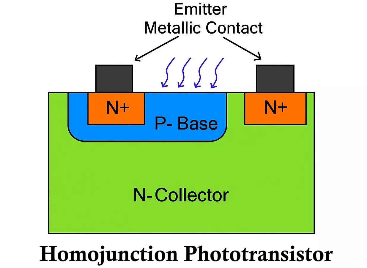
Key features:
- Fabricated entirely from one material (e.g. Si or GaAs).
- Energy bandgap is uniform across the device.
- Typically cheaper to fabricate.
- Lower sensitivity than heterojunction due to recombination losses.
Design:
- Optimized base thickness for light penetration.
- Surfaces and junctions are passivated to reduce recombination losses.
- Structure usually like a regular BJT but packaged with a transparent top window.
Heterojunction Phototransistor
A heterojunction phototransistor uses different semiconductor materials with different bandgaps for the emitter, base, and collector.
(e.g. GaAs/AlGaAs, InP/InGaAs)
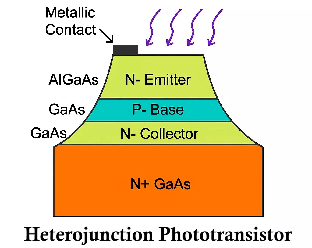
Key features:
- Improved gain and sensitivity due to better carrier confinement.
- Higher bandwidth and faster response due to material optimization.
- Lower dark current and noise.
- Often used for long-wavelength IR phototransistors and specialized optical communications.
Design:
- Lattice matching to reduce defects at junction.
- Graded bandgap profiles to improve carrier injection.
- Often more expensive to produce but deliver higher performance.
Comparison Table
Here is a simple comparison of homojunction and heterojunction phototransistors.
| Feature | Homojunction | Heterojunction |
|---|---|---|
| Semiconductor Material | Single type | Multiple types |
| Bandgap | Uniform | Varies across layers |
| Performance | Moderate gain | Higher gain & speed |
| Complexity | Simpler | More complex |
| Typical Applications | General-purpose light sensing | Fiber optics, IR detection, high-speed applications |
Working of Phototransistor
A phototransistor operates on the principle of photoconductivity combined with transistor action:
- Incident Light: When light strikes the phototransistor’s base-collector junction, it generates electron-hole pairs.
- Base Current: The generated carriers act as a tiny base current, turning on the transistor.
- Current Amplification: Due to the transistor’s gain (h_FE), even small light-induced base currents produce much larger collector currents.
- Output Signal: The resulting current at the collector is a highly amplified version of the incident light intensity, allowing light sensing with a much higher sensitivity than a photodiode.
Key Equation:
IC ≈ β × Iphoto
Where:
- IC = Collector current
- β = DC current gain of the phototransistor
- Iphoto = Photogenerated base current
Modes of Operation
Linear or Active Mode
- The phototransistor operates as an analog amplifier.
- Output current is proportional to light intensity.
- Practically, this relation is nonlinear, so this region is often called active mode.
- Base current generated by light is amplified by the transistor’s gain.
- Applications: Amplification of light signals, analog light measurements.
Switch Mode
- Phototransistor behaves like a digital switch — only two states:
- “Off” state (no light → no current).
- “On” state (enough light → saturated output current).
- When light intensity passes a threshold, output saturates.
- Applications: Object detection, light barriers, optical signal decoding, level switching.
Circuit Configurations of Phototransistor
Common-Emitter Configuration
- Collector is connected to a power source via a load resistor (Rc).
- Output is taken from the collector.
- Output voltage drops (goes low) when light is detected.
- Widely used for amplification and switching.
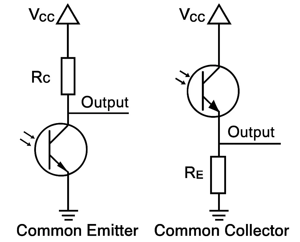
Common-Collector (Emitter-Follower) Configuration
- Emitter is connected to ground through a load resistor (RE).
- Output is taken from the emitter.
- Output voltage rises (goes high) as light is detected.
- Provides current gain without much voltage gain — acts as a buffer.
Types of Phototransistors
Phototransistors come in various types and configurations to suit different application requirements:
BJT Phototransistors
- Built with bipolar junction transistors (BJT) as the light-sensing element.
- Available in NPN and PNP versions.
- When light strikes the base region, it generates a small base current that is amplified into a larger collector current.
- Good for general-purpose phototransistor circuits, though they have leakage current in dark and lower high-frequency response.
Two-Lead Phototransistor (Collector, Emitter)
- Base is internally left floating.
- Common in most optoelectronic switch designs.
- Simplifies usage since no separate base terminal is needed.
Three-Lead Phototransistor (Collector, Base, Emitter)
- Allows an external bias to the base.
- Provides greater flexibility for control and sensitivity tuning.
Darlington Phototransistors
- Consist of two transistors in a Darlington pair.
- Offer very high current gain, making them ideal for very low light levels.
NPN and PNP Phototransistors
- NPN types: More common due to faster response and higher gain.
- PNP types: Available for complementary designs.
FET Phototransistors
- Built using field-effect transistors (FET) that feature a light-sensitive channel.
- Have Source and Drain terminals; the light intensity modulates the current between them.
- Offer higher switching speed and better high frequency operation but produce lower output currents and gains compared to BJT phototransistors.
Parameters and Characteristics of Phototransistors
Device Overview
A phototransistor is fundamentally similar to a BJT, except that its base is light-controlled. It typically has only two terminals — Collector (C) and Emitter (E) — with the base left floating. Some phototransistors may provide an accessible base terminal, which must usually remain disconnected for light-sensitive operation.
- The collector is biased at a higher potential than the emitter.
- Under no-light conditions, a small leakage current (dark current) still flows.
- Incident light on the base region generates a base current proportional to light intensity. This current is then amplified to produce a large collector current.
Two Operating Modes
- Active Mode — Amplifies the photocurrent proportional to light intensity.
- Switch Mode — Operates digitally as “off” (no light) or “on” (saturated) when light reaches a threshold.
Performance Parameters
Key parameters that influence phototransistor performance:
- Collector Current (IC): Maximum allowed load current. Exceeding this can cause permanent damage.
- Base Current: Generated by light intensity; larger base area yields higher sensitivity but higher capacitance and slower response.
- Dark Current (ID): Leakage current present with no light — dependent on temperature.
- VCE Breakdown Voltage: Maximum collector–emitter voltage before breakdown.
- VEC Breakdown Voltage: Maximum emitter–collector voltage; usually much lower than VCE breakdown.
- Wavelength Range: Phototransistors are most sensitive at specific wavelengths:
- Silicon: 190–1100 nm
- Germanium: 400–1700 nm
- InGaAs: 800–2600 nm
- Lead sulfide (PbS): 1000–3500 nm
- Linearity: Indicates how linearly output current scales with light intensity — higher is better.
- Sensitivity: Ratio of change in output current per unit change in light intensity.
- Response Time: Time to respond to variations in light intensity.
- Rise/Fall Time: Time for output to rise (10%–90%) or fall (90%–10%). Smaller is better for fast response.
- Size and Cost: Smaller, inexpensive phototransistors are more economical for commercial designs.
Design Parameters
Material and structure greatly affect performance:
- Homojunction Structure:
- Single semiconductor material (e.g. silicon).
- Easier fabrication, gain typically tens to hundreds.
- Heterojunction Structure:
- Layers of different semiconductor materials.
- Achieves very high sensitivity (gain up to 10,000) but complex and costly.
- Material Selection: Determines wavelength response:
Collector Characteristics
The VCE – IC curve of a phototransistor looks like a BJT output characteristic, with different light intensity levels plotted as separate curves:
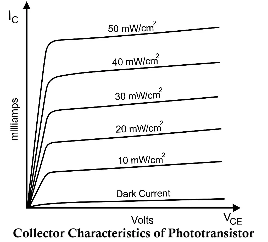
- X-Axis: VCE (Voltage between collector and emitter)
- Y-Axis: IC (Collector current)
- Higher light intensity → larger IC at the same VCE.
- Even with no light, there is a small dark current present.
Spectral Response
Spectral response describes how the phototransistor’s sensitivity varies with the wavelength of light:
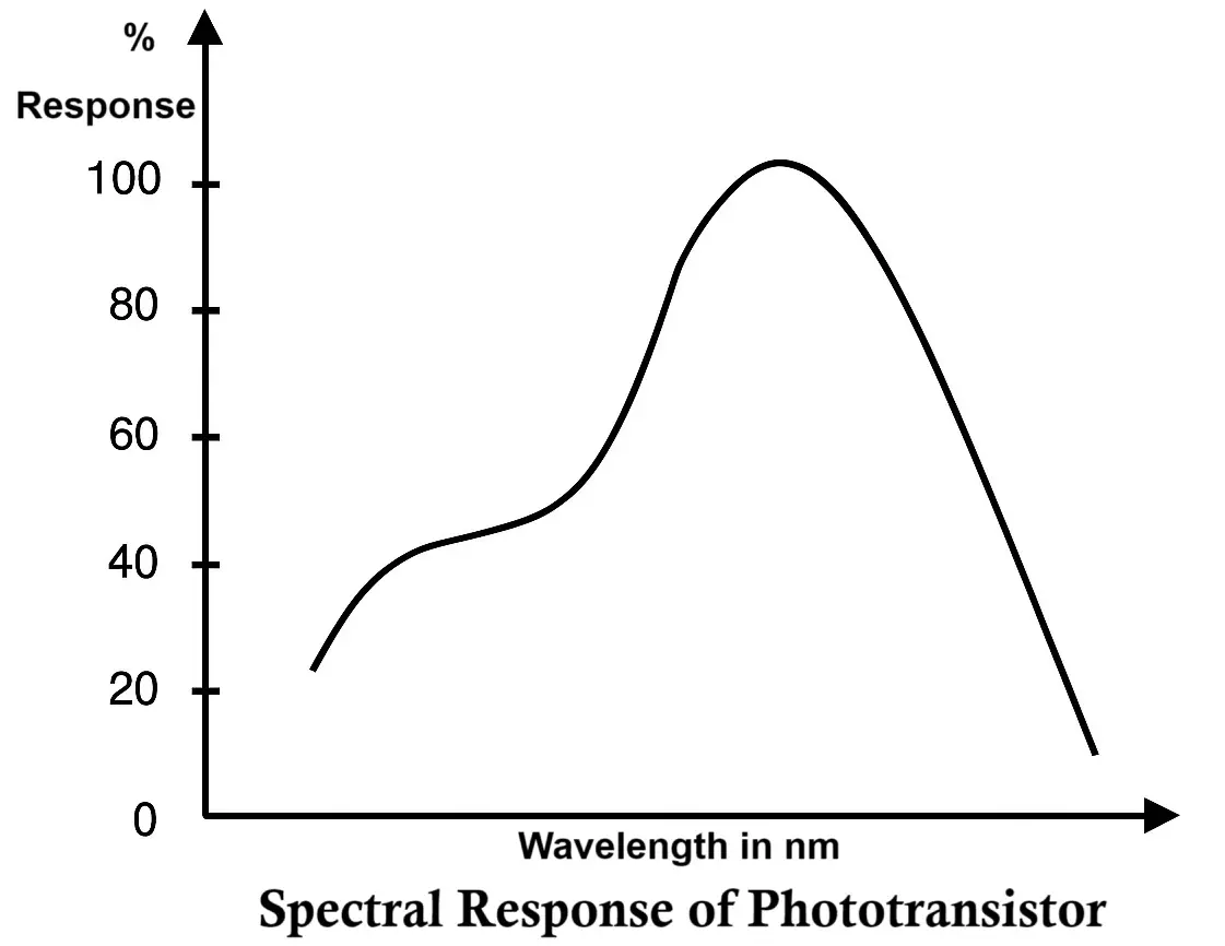
- Phototransistors have a peak response in a narrow range of wavelengths.
- Efficiency and sensitivity drop off outside this optimal band.
Switching Speed
Due to the relatively large junction and base-collector capacitance, phototransistors have limited bandwidth (typically up to 250 kHz). This restricts them to low- to mid-speed applications like light sensing, opto-isolation, object detection, and remote-control decoding.
Advantages of Phototransistors
- High sensitivity to light – much higher than photodiodes due to internal current gain.
- High current gain, especially in heterojunction designs, allowing amplification of very small light signals to a large output current.
- Simple, small, light-weight, compact, and inexpensive – easy to manufacture and integrate into circuits and ICs.
- Direct light-to-current conversion simplifies interfacing with analog or digital electronics.
- Sensitive to a broad range of wavelengths – from ultraviolet through visible to infrared.
- Low noise and stable operation under normal conditions.
- Acts as both a light sensor and an amplifier.
- Able to sense light from diverse sources – sunlight, flames, incandescent lamps, lasers, IR LEDs, etc.
- Reliable and energy-efficient, making them ideal for long-term, low-power sensing.
Disadvantages of Phototransistors
- Slower response and limited bandwidth (~250 kHz max), due to high junction capacitance.
- Not suitable for high-speed or RF applications, making them slower than photodiodes.
- More susceptible to dark current – leakage current that increases with temperature, causing false output.
- Cannot detect extremely low light levels without noise interference.
- Voltage surges and spikes can easily damage them due to limited breakdown voltages.
- Lower voltage and power handling capacity than devices like thyristors or TRIACs.
- Nonlinear response – output is not perfectly proportional to light intensity.
- Sensitive to electromagnetic interference (EMI), which can cause spurious switching.
- Mostly sensitive to IR and visible light, special variants needed for other wavelengths.
- Saturation at high light intensity, limiting dynamic range.
Applications of Phototransistors
Phototransistors are highly useful in a range of light-sensing and optoelectronic applications:
- Optical switches: Detecting light interruptions in automation and control systems.
- Light-activated relays: Switching devices on or off when light intensity changes.
- Optical encoders & Tachometers: Sensing light pulses for rotation or position measurements in robotics and industrial machines.
- Object detection and counting: Common in conveyor belts and assembly lines.
- Optocouplers (optical isolation): Electrically isolating different sections of a circuit for safety and noise immunity.
- Automatic lighting control: Streetlights, emergency lighting, and home automation.
- Smoke and fire detectors: Detecting light scattering from smoke particles.
- Remote control receivers: Receiving infrared signals from handheld remote devices.
- Optical communication: Data transfer using light, especially in simple or low-speed systems.
- Burglar alarms and safety systems: Detecting intrusions or obstructions using light beams.
- Automatic door openers: Sensing a person or object to trigger door operation.
- Paper and tape readers: Detecting light and dark patterns for data encoding.
- Non-contact position sensing: Detecting presence or movement without physical contact.
- Street Lighting Systems: Automatic on-off control based on light.
- Barcode Scanners & Optical Sensors: Reading patterns and printed codes.
Conclusion
Phototransistors bridge the worlds of optics and electronics by utilizing light as an input and generating an amplified electrical output. Thanks to their simple operation, high sensitivity, and ease of use, phototransistors have become fundamental components across a broad range of automation, communication, and sensing technologies. TEMT6000, L14F1, L14G2 and BPW77 are some of the very popular phototransistors.
They offer an economical and efficient means of detecting light with greater sensitivity than photodiodes, making them ideal for detecting small light levels and obtaining a significant output current.
What is a Sensor? Types of Sensors, Classification & Applications
Light Dependent Resistor (LDR) / Photoresistor Circuit Diagram & Working
Piezoelectric Transducer – Construction, Working and Applications
