In today’s world, most electronic devices operate digitally, but the signals we experience in the real world—such as sound, light, temperature, and pressure—are analog in nature. To process these signals in microcontrollers, digital signal processors (DSPs), or computers, we need to convert analog signals into digital form. This is where an Analog-to-Digital Converter (ADC) comes into play. An ADC is an essential building block in embedded systems, digital communication, audio/video processing, measurement instruments, and countless other fields.
What is an Analog to Digital Converter (ADC)?
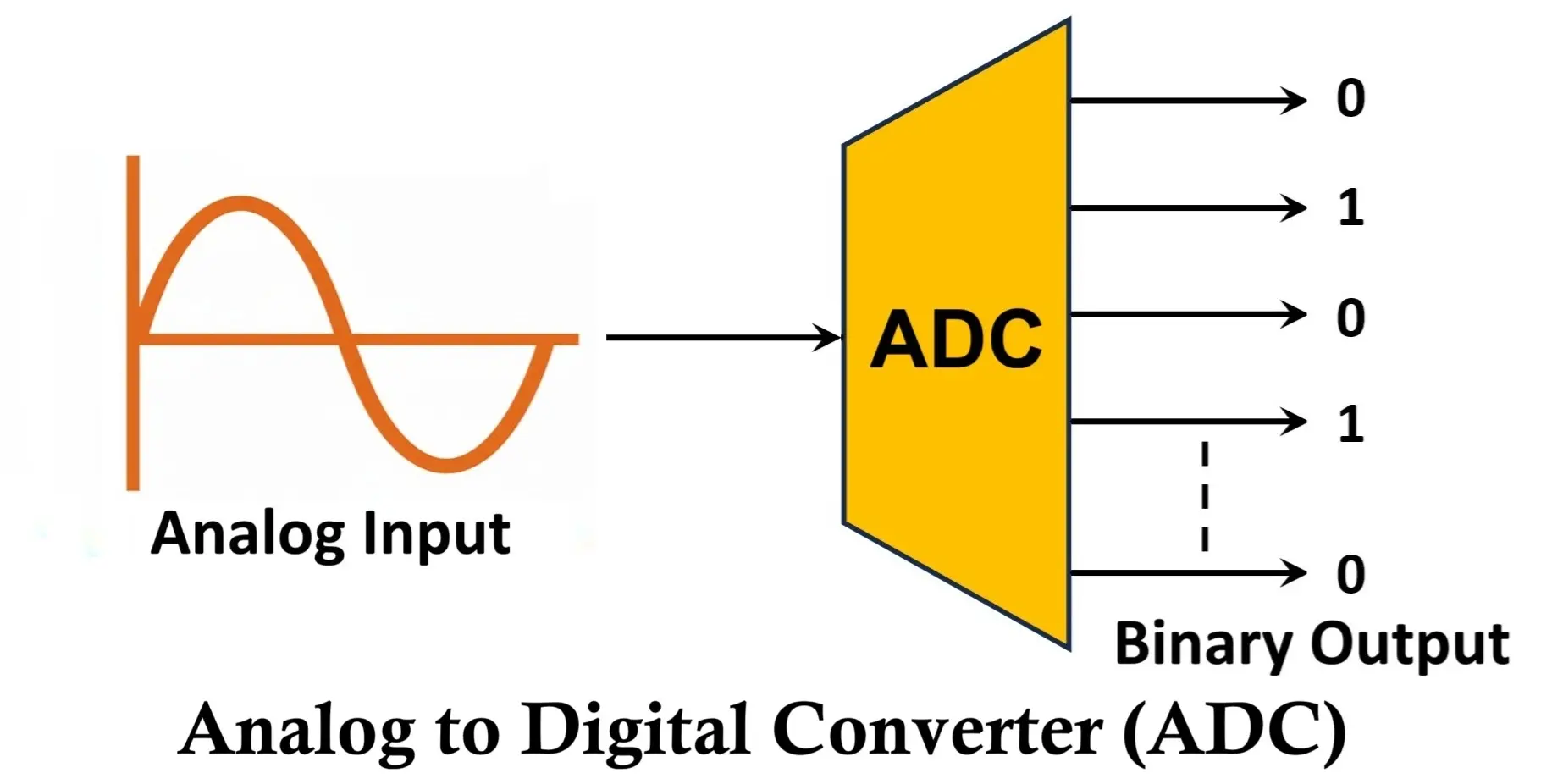
An Analog-to-Digital Converter (ADC) is an electronic circuit that converts a continuous-time, continuous-amplitude analog signal into a discrete-time, discrete-amplitude digital signal. The output is usually in binary form, which digital systems can store, process, or transmit.
For example:
- A microphone generates an analog audio signal.
- An ADC samples this signal and converts it into a sequence of binary values.
- These binary values can then be processed by a microcontroller, computer, or DSP to create same audio.
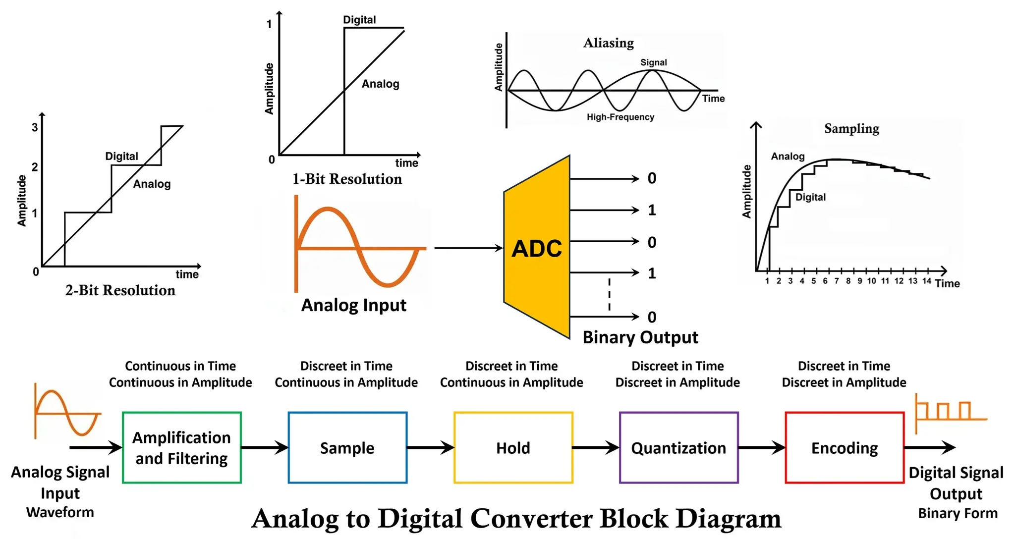
Block Diagram of Analog to Digital Converter ADC
Here’s a detailed explanation of the block diagram of an ADC:
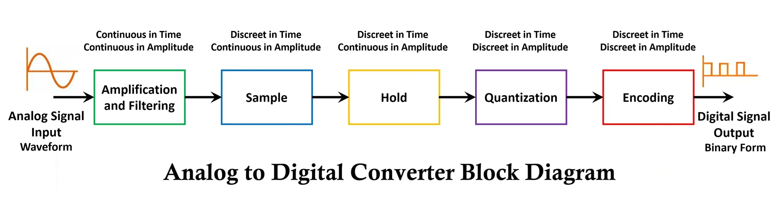
1. Analog Input
- This is the continuous-time analog signal (e.g., microphone voltage, sensor output).
- It can have infinite values within a given range, so the ADC must process it into finite discrete steps.
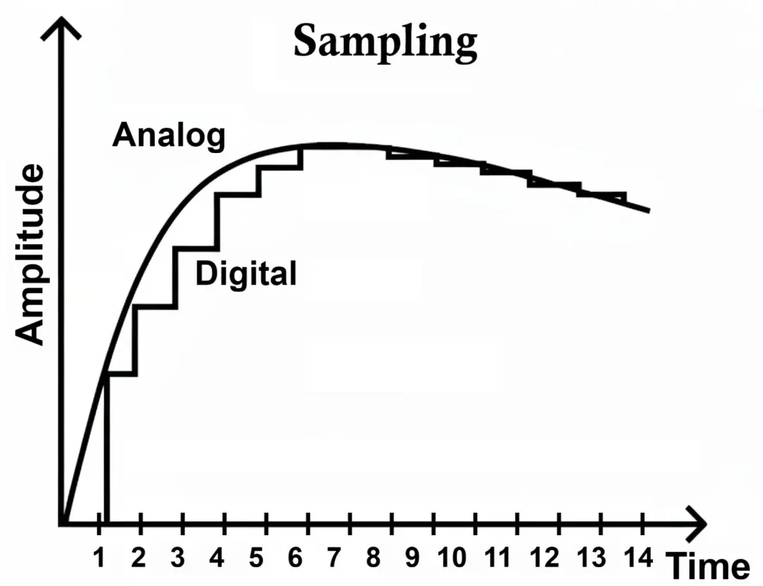
2. Sample and Hold Circuit (S/H)
- Real-world analog signals are continuously varying. To convert them, we first sample the signal at regular time intervals.
- The Sample part takes “snapshots” of the signal at discrete time instants, determined by the sampling frequency (must follow Nyquist theorem: sampling frequency ≥ 2 × max signal frequency).
- The Hold part keeps the sampled value constant for a short duration so the next stage (quantizer) can process it.
- This prevents errors due to signal variation during conversion.
3. Quantizer
- The sampled signal is continuous in amplitude. The quantizer maps it into a finite set of discrete levels (steps).
- For example, in an 8-bit ADC, there are 28 = 256 levels.
- This introduces quantization error (difference between actual input and quantized value), which is inherent in all ADCs.
- The smaller the step size (Δ), the higher the resolution and accuracy.
4. Encoder (Binary Encoder)
- The quantized levels are then encoded into a digital binary number.
- For instance, if an ADC has 3 bits, it can represent values in the range 000 to 111 (0–7 in decimal).
- The encoder outputs the final digital representation of the analog input.
5. Digital Output
- The final stage gives a digital binary code corresponding to the input analog signal.
- This output can be processed by microcontrollers, DSPs, or computers.
- Typically represented in n-bit resolution (e.g., 8-bit, 10-bit, 12-bit, 16-bit ADC).
Supporting Blocks (sometimes included in detailed diagrams):
- Clock Circuit: Provides timing signals to the sample & hold and conversion process.
- Comparator(s): Used in successive approximation or flash ADCs to compare input with reference voltages.
- Reference Voltage (Vref): Defines the maximum and minimum conversion range.
Flow Summary
- Analog input signal applied.
- Sample & hold captures and stabilizes signal.
- Quantizer converts amplitude into nearest discrete level.
- Encoder converts level into binary code.
- Digital output is available for digital processing.
Example:
- Suppose we have a 3-bit ADC with a range of 0–8 V.
- Step size Δ = Vrange/2N = 8/23 = 1V.
- Input = 5.3 V → quantized to 5 V → binary output =
101.
Performance Factors of ADC
Here are the key performance factors that determine how well an ADC works. Let’s go through each one in detail:
1. Resolution
- Definition: The number of bits used to represent the analog input in digital form.
- An N-bit ADC divides the input range into 2^N discrete levels.
- Higher resolution → more accurate conversion.
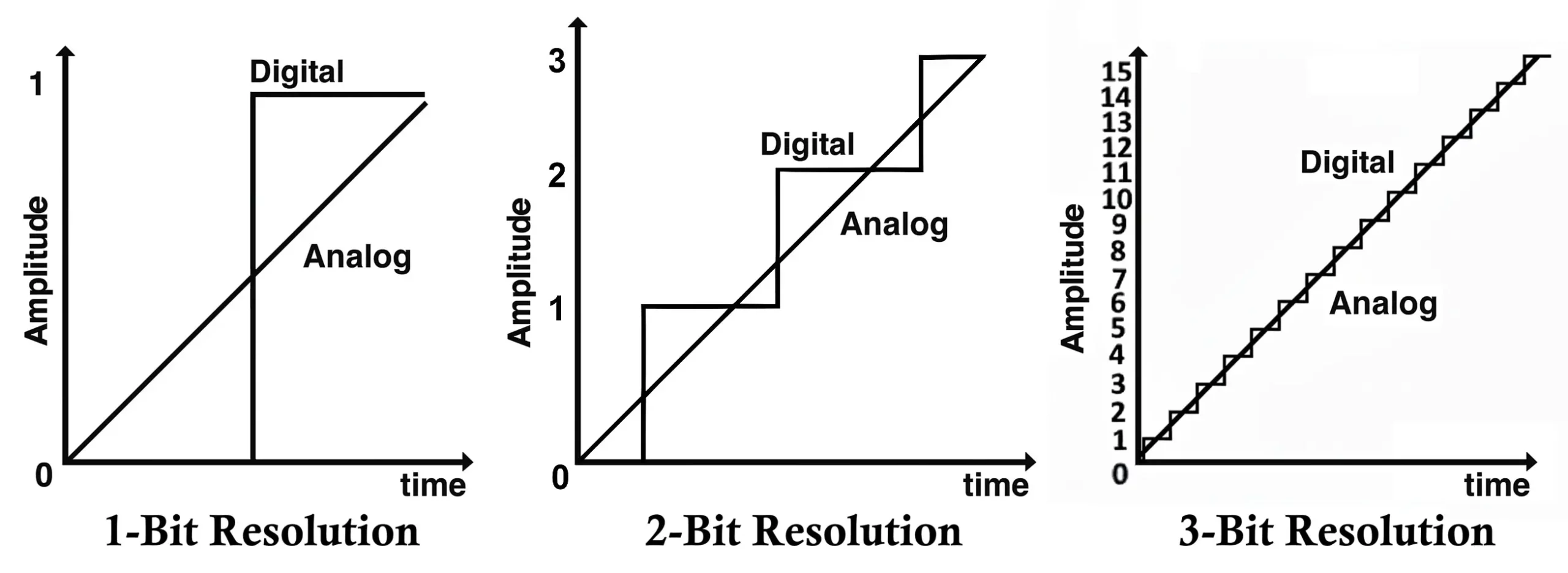
- Example:
- 3-bit ADC → 8 levels
- 8-bit ADC → 256 levels
- 12-bit ADC → 4096 levels
2. Width of the Step (Step Size / LSB)
- Definition: The minimum change in input voltage that can cause a change in the output digital code.
Formula: Δ = Vref/2N
where, Vref = reference voltage, N = number of bits.
Example: 8-bit ADC with Vref = 5V
Δ = 5/256 ≈ 19.53 mV
3. Quantization Error
- Definition: The error between the actual analog input and the nearest quantized level.
- It arises because continuous signals are mapped to discrete values.
- Maximum quantization error = ±(½ step size).
- Example: If step size = 20 mV, quantization error = ±10 mV.
4. Sampling Rate
- Definition: The rate at which the analog signal is sampled per second (samples/sec).
- If the sampling rate is too low, signal information is lost.
- Typical unit: Hz (or kHz, MHz).
- Controlled by a sampling clock.
5. Aliasing
- Definition: When the input signal contains frequencies higher than half the sampling rate, these frequencies are misrepresented as lower frequencies in the digital output.
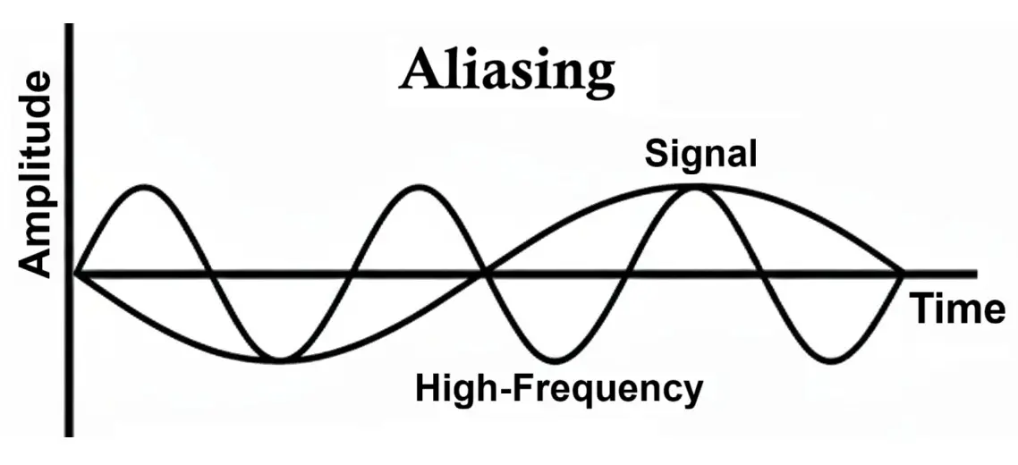
- This causes distortion (wrong frequency components).
- Solution: Use an anti-aliasing filter (low-pass filter before ADC) to remove high-frequency components.
6. Nyquist Criteria
- Definition: To avoid aliasing, the sampling frequency (fs) must be at least twice the maximum signal frequency (fmax).fs ≥ 2fmax
- Example: If the signal has a maximum frequency of 10 kHz, the sampling rate should be ≥ 20 kHz.
7. Offset (Offset Error)
- Definition: The difference between the actual ADC output and the ideal output when the input is zero volts.
- Ideally, 0 V input → digital output = 000…0.
- But due to imperfections, a small error appears (e.g., digital code = 001 when input is 0 V).
- This is called offset error.
In summary:
- Resolution → number of digital steps.
- Step size → voltage difference between two steps.
- Quantization error → inevitable rounding error.
- Sampling rate → how often we measure.
- Aliasing → false frequency if Nyquist not followed.
- Nyquist criteria → must sample at least twice max frequency.
- Offset → error at 0 input.
Types of Analog to Digital Converters (ADC)
Converting continuous analog signals (like sound, temperature, or voltage) into discrete digital values that can be processed by microcontrollers or digital systems is very important. The choice of ADC depends on speed, accuracy, resolution, cost, and power consumption. Here are the main types of ADCs explained in detail:
1. Flash ADC (Parallel ADC)
- Working principle: Uses a bank of comparators to compare the input voltage with a set of reference voltages simultaneously. The outputs are then encoded into a binary number.
- Speed: Extremely fast (nanoseconds).
- Resolution: Limited (typically up to 8 bits) because the number of comparators doubles with each additional bit (e.g., 8-bit needs 255 comparators).
- Applications: Digital oscilloscopes, radar systems, video processing, and high-frequency communication.
- Advantages: Fastest ADC architecture, low latency.
- Disadvantages: High power consumption, expensive, impractical for high resolutions.
2. Successive Approximation Register (SAR) ADC
- Working principle: Uses a comparator and a digital-to-analog converter (DAC) in a feedback loop. The SAR logic tests each bit one by one (from MSB to LSB) to find the closest digital match to the input voltage.
- Speed: Moderate (microseconds).
- Resolution: High (8–16 bits commonly).
- Applications: Industrial control, instrumentation, microcontrollers, medical devices.
- Advantages: Good trade-off between speed, resolution, and cost; low power consumption.
- Disadvantages: Slower than flash ADCs.
3. Sigma-Delta (ΔΣ) ADC
- Working principle: Oversamples the input signal at a very high rate and uses noise shaping + digital filtering to achieve high resolution. It integrates the input over time and produces a high-resolution digital output after decimation.
- Speed: Low (kHz range).
- Resolution: Very high (16–24 bits).
- Applications: Audio systems (CD/DVD players, studio equipment), precision measurement instruments.
- Advantages: Excellent resolution and accuracy, good for low-frequency signals.
- Disadvantages: Slow response, unsuitable for high-speed applications.
4. Dual-Slope (Integrating) ADC
- Working principle: First, the input voltage is integrated for a fixed time, then a reference voltage of opposite polarity is applied until the integrator returns to zero. The time taken is proportional to the input voltage.
- Speed: Slow (milliseconds).
- Resolution: High (12–16 bits).
- Applications: Digital multimeters, weighing machines, instrumentation.
- Advantages: Very accurate, excellent noise rejection.
- Disadvantages: Very slow, not suitable for fast-changing signals.
5. Pipeline ADC
- Working principle: Breaks down the conversion process into stages (pipeline). Each stage converts part of the signal and passes the residue to the next stage until the final result is assembled.
- Speed: High (tens to hundreds of MSPS – Mega Samples Per Second).
- Resolution: Medium to high (8–16 bits).
- Applications: Video processing, wireless communication, medical imaging.
- Advantages: Good compromise between speed and resolution, scalable.
- Disadvantages: Higher latency compared to flash ADC, complex design.
6. Time-Interleaved ADC
- Working principle: Uses multiple ADCs working in parallel but staggered in time. Their outputs are interleaved to achieve a higher effective sampling rate.
- Speed: Extremely high.
- Resolution: Depends on the individual ADCs used.
- Applications: Ultra-fast communication systems, radar, high-speed data acquisition.
- Advantages: Very high throughput.
- Disadvantages: Requires calibration to handle timing mismatches and distortions.
7. Semi-Flash (Two-Step) ADC
- Working principle: Splits the conversion into two stages to reduce the number of comparators. The first stage makes a coarse conversion (most significant bits), and the second stage refines the result with fewer comparators than a full flash ADC.
- Speed: High (faster than SAR, slower than pure flash).
- Resolution: Moderate to high (8–12 bits) without needing hundreds of comparators.
- Applications: Medium- to high-speed data acquisition, video, communication systems.
- Advantages: Faster than SAR, fewer comparators than flash, good compromise.
- Disadvantages: More complex than SAR, not as fast as pure flash.
8. Counting (or Ramp) ADC
- Working principle: Uses a counter and DAC. The counter increases until the DAC output matches the input analog voltage (checked by a comparator).
- Speed: Very slow.
- Resolution: Moderate (depends on counter size).
- Applications: Simple instrumentation, low-cost systems.
- Advantages: Simple design, low cost.
- Disadvantages: Very slow, not used in modern high-speed systems.
Each ADC architecture has its own construction style, but the core components— Sample & Hold, Quantizer, and Encoder — remain the same.
Advantages of Analog to Digital Converter (ADC)
- Digital Compatibility: ADCs convert analog signals into digital form, allowing them to interface with microcontrollers, computers, and digital processing systems for analysis, control, and storage.
- Noise Immunity: Once converted to digital, the signal is much less affected by noise, making long-distance transmission more reliable compared to analog signals.
- Easy Storage and Reproduction: Digital signals can be stored in memory without loss of quality and reproduced accurately, unlike analog signals which degrade over time.
- Precision and Accuracy: High-resolution ADCs can measure analog signals with fine detail, enabling precise control in applications like instrumentation and automation.
- Support for Digital Signal Processing: Once converted, the signal can be filtered, compressed, or analyzed using digital algorithms, enabling advanced processing capabilities.
Disadvantages of Analog to Digital Converter (ADC)
- Limited Resolution: ADCs represent continuous signals in discrete steps. This quantization introduces small errors, meaning the digital signal is only an approximation of the original analog input.
- Sampling Limitations: ADCs sample signals at specific rates. If the input frequency is too high relative to the sampling rate, aliasing occurs, causing distortion in the digital representation.
- Complexity and Cost: High-speed or high-resolution ADCs require sophisticated design and are more expensive, increasing the overall system cost.
- Conversion Delay (Latency): The process of converting an analog signal to digital takes time, which can introduce delays in real-time applications.
- Power Consumption: ADCs, especially high-speed types, can consume significant power, which is critical in battery-operated or low-power devices.
- Input Range Limitations: ADCs can only accept signals within a specific voltage range. Signals outside this range need conditioning (amplification or attenuation), adding complexity.
Applications of Analog to Digital Converter (ADC)
ADCs are everywhere in modern electronics. Some important applications include:
- Digital Audio Systems: ADCs convert analog audio signals from microphones or instruments into digital form for processing, storage, or transmission in devices like smartphones, music players, and recording equipment.
- Digital Imaging: In cameras and scanners, ADCs convert analog light signals captured by sensors into digital images that can be stored, edited, and transmitted.
- Medical Instrumentation: ADCs are used in devices like ECG, EEG, and digital thermometers to convert physiological signals into digital data for monitoring, analysis, and diagnosis.
- Industrial Automation: Sensors in industrial systems produce analog signals such as temperature, pressure, or flow, which ADCs convert to digital signals for process control, monitoring, and automation.
- Communication Systems: ADCs convert analog signals in radio, television, and telecommunication systems into digital signals for modulation, transmission, and digital processing.
- Data Acquisition Systems: ADCs are essential in scientific research and engineering to digitize analog signals from experiments, tests, or sensors for recording, analysis, and modeling.
- Consumer Electronics: ADCs are used in devices like digital thermometers, game controllers, and touchscreens to convert analog inputs (temperature, pressure, touch) into digital data for processing.
- Instrumentation and Measurement: ADCs enable precise digital measurement of analog quantities in voltmeters, oscilloscopes, and multimeters for monitoring and analysis.
- Automobiles: ADCs convert analog signals from sensors like speed, engine temperature, fuel level, and oxygen sensors into digital data for engine control units (ECUs), safety systems, and advanced driver-assistance systems (ADAS).
Conclusion
An Analog-to-Digital Converter (ADC) acts as a crucial interface between the analog real world and the digital domain of modern electronics. By converting continuous signals into discrete binary codes, ADCs make it possible for digital systems to process, analyze, and control real-world phenomena. ADS115, MCP3004 and HX711 are some of the popular ADCs/modules often used with Arduino.
With various architectures like Flash, SAR, Dual-Slope, and Sigma-Delta, ADCs can be optimized for speed, resolution, or accuracy, depending on the application. Despite minor limitations such as quantization error and aliasing, ADCs are indispensable in almost every modern electronic device—from smartphones and automobiles to medical equipment and scientific instruments.
Digital to Analog Converter (DAC) Block Diagram, Working, Types & Applications