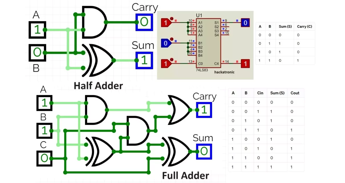
Let’s see half and full adder truth table with circuit diagram and its working. Also, we have implemented it using 7483 IC. Let’s start with the half adder.
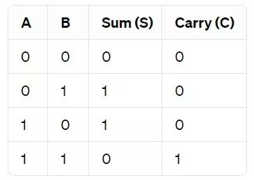
Half Adder Truth table and Circuit Design:
A half adder is a digital circuit that performs the addition of two single binary digits A and B. It produces two outputs: the sum (S) and the carry (C). Here’s the truth table for a half adder:
Now, let’s represent this with a circuit diagram and the logic gates involved:
Circuit Diagram:
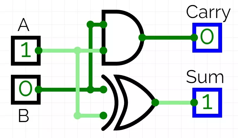
Explanation:
- A and B are inputs.
- The AND gate produces the carry out (C).
- The XOR gate produces the sum (S).
K Map for Half Adder
we can see that the expressions for Sum (S) and Carry (C) are already in their simplest forms, and no further simplification is possible. This is because the truth table of a half adder is straightforward and does not require complex logic. Therefore, K-maps are not typically utilized for half adders due to their simplicity.
Logical Expression for Half Adder
Sum (S): The sum (S) is obtained using the XOR gate logic, which produces a ‘1’ output when the number of ‘1’s in the inputs is odd.
S = A ⊕ B
Carry (C): The carry (C) is obtained using the AND gate logic, which produces a ‘1’ output only when both inputs are ‘1’s.
C = A.B
So, the logical expressions for the half adder are:
- Sum (S) = A ⊕ B
- Carry (C) = A.B
These expressions describe how the outputs of a half adder are derived based on the inputs A and B.
VHDL Code for a Half Adder:
-- Half Adder VHDL code

library IEEE;
use IEEE.STD_LOGIC_1164.ALL;

entity half_adder is
Port ( A : in STD_LOGIC;
B : in STD_LOGIC;
Sum : out STD_LOGIC;
Carry : out STD_LOGIC );
end half_adder;

architecture Behavioral of half_adder is
begin
Sum <= A XOR B; -- Sum is the XOR of A and B
Carry <= A AND B; -- Carry is the AND of A and B
end Behavioral;
Explanation:
- This VHDL code defines a half adder entity with inputs A and B and outputs Sum and Carry.
- In the architecture section, the Sum output is defined as the XOR of inputs A and B, and the Carry output is defined as the AND of inputs A and B.
You can simulate this code using a VHDL simulator or synthesize it for FPGA or ASIC implementation.
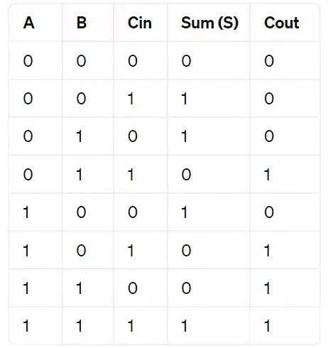
Full Adder Truth table and Circuit Design:
A full adder is a combinational circuit that performs the arithmetic sum of three input bits: A, B, and an input carry (Cin). It produces two outputs: the sum (S) and the carry out (Cout). Here’s the truth table for a full adder:
Now, let’s represent this with a circuit diagram and the logic gates involved:
Circuit Diagram:
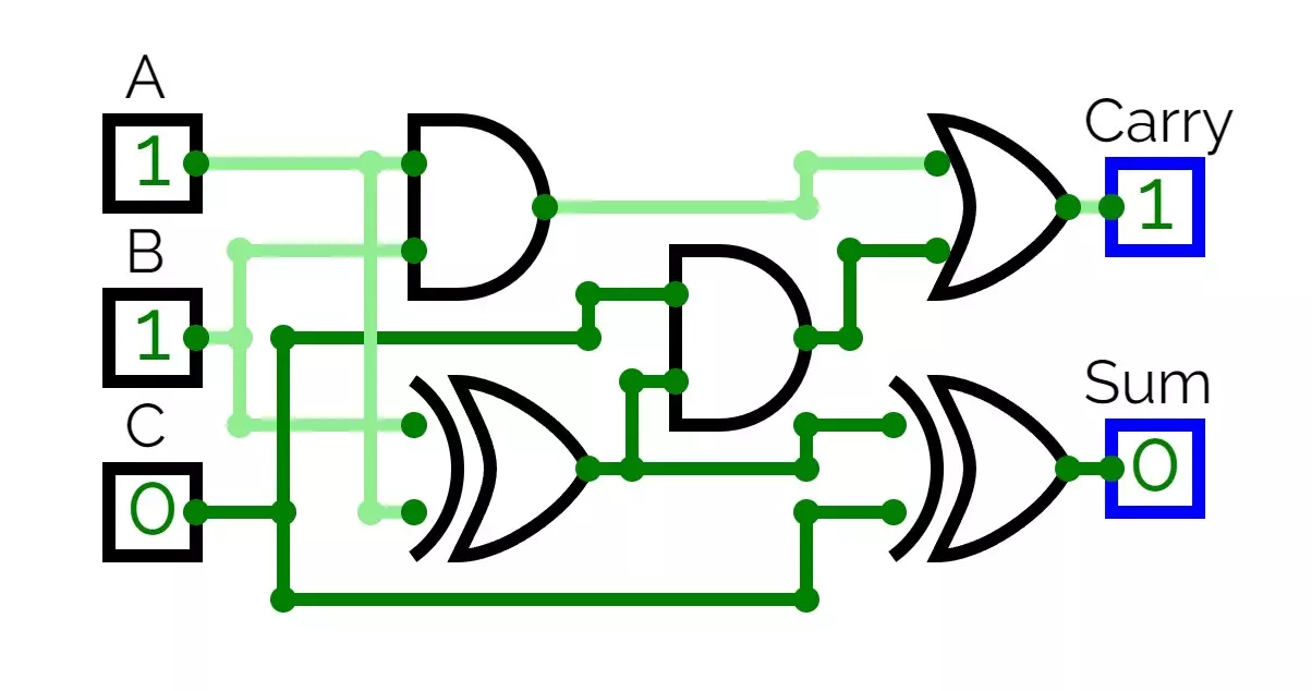
Explanation:
A, B, and Cin are the inputs.
The XOR gate produces the sum (S).
The AND gate produces the carry out (Cout).
OR gates are used to combine different inputs.
This is how half adders and full adders work, and these circuits are fundamental building blocks in digital electronics, forming the basis for more complex arithmetic operations.
K Map for Full Adder
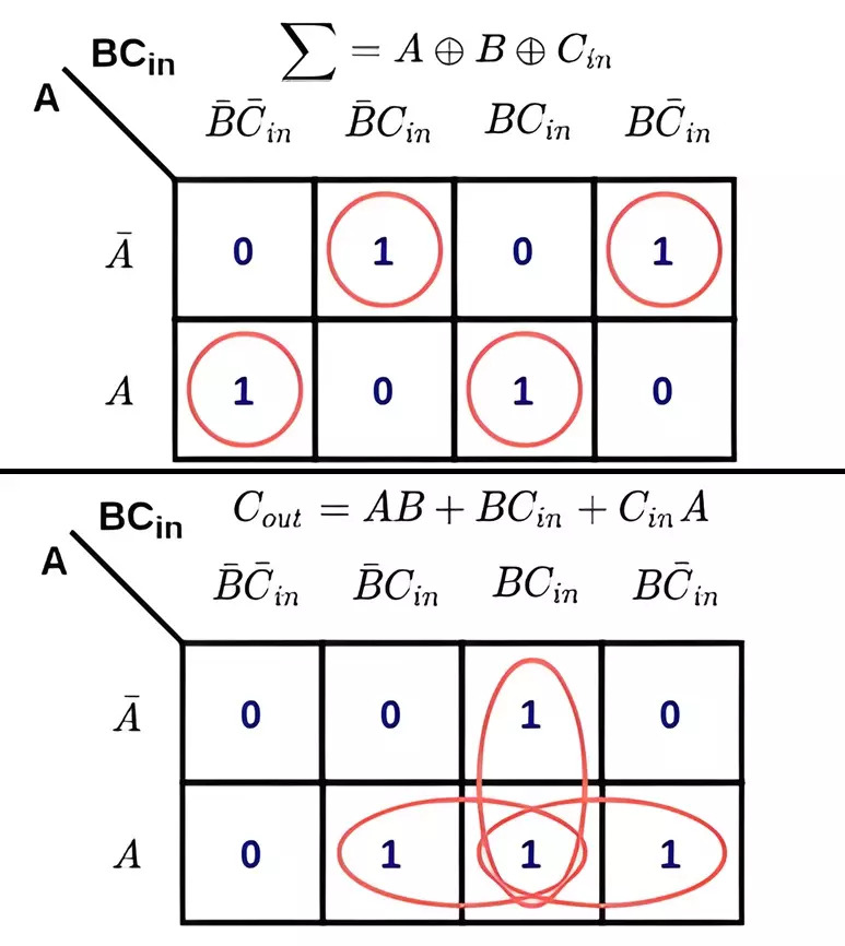
From the Karnaugh maps,
Simplified Expression for Sum (S):
S = A’B’Cin + A’BCin’ + AB’Cin’ + ABCin
Simplified Expression for Carry (Cout):
Cout = A’B + AB’Cin + A’Cin + BCin
These simplified expressions represent the logic functions of the full adder, derived from the Karnaugh maps. They provide a minimized representation of the Boolean expressions for both the sum and carry outputs of the full adder circuit.
Logical Expression for Full Adder
A full adder adds three input bits: A, B, and a carry-in (Cin), and produces two outputs: the sum (S) and the carry-out (Cout).
The logical expressions for the sum (S) and carry-out (Cout) in terms of A, B, and Cin can be written as follows:
Sum (S) Expression:
S = A ⊕ B ⊕ Cin
Carry-Out (Cout) Expression:
Cout = A.B + B.Cin + A.Cin
These expressions capture the behavior of a full adder, allowing you to implement it using logic gates or integrated circuits.
VHDL Code for a Full Adder:
-- Full Adder VHDL code
library IEEE;
use IEEE.STD_LOGIC_1164.ALL;

entity full_adder is
Port ( A : in STD_LOGIC;
B : in STD_LOGIC;
Cin : in STD_LOGIC;
Sum : out STD_LOGIC;
Cout : out STD_LOGIC);
end full_adder;

architecture Behavioral of full_adder is
begin
process(A, B, Cin)
begin
Sum <= (A xor B) xor Cin; -- XOR operation for sum
Cout <= (A and B) or (Cin and (A xor B)); -- OR operation for carry out
end process;
end Behavioral;
Explanation
entity full_adder: This defines the interface of the full adder, specifying its input and output ports.architecture Behavioral: This is the implementation part of the full adder.- Inside the
processblock, the behavior of the full adder is defined based on the inputs A, B, and Cin. Sum <= (A xor B) xor Cin;: This line computes the sum output by performing XOR operations between A and B, and then XORing the result with Cin.Cout <= (A and B) or (Cin and (A xor B));: This line computes the carry output. It involves AND and OR operations on the inputs A, B, and Cin.STD_LOGICis the standard logic type used in VHDL for representing digital signals. It has four values: ‘0’, ‘1’, ‘Z’ (high-impedance), and ‘X’ (unknown).xoris the XOR operator, andand,orare logical operators in VHDL.
This code implements the behavior of a full adder in VHDL, which adds three binary inputs (A, B, and Cin) and produces two outputs (Sum and Cout).
You can simulate this code using a VHDL simulator or synthesize it for FPGA or ASIC implementation.
Difference between Half Adder and Full Adder:
The main difference between a half adder and a full adder lies in their capabilities to handle carry inputs from previous addition stages. You can see in half and Full adder truth table.
Half Adder:
- A half adder is a digital circuit that adds two single binary digits.
- It produces two outputs: the sum (S) and the carry (C).
- It does not take into account any carry from previous addition stages.
- Therefore, it’s suitable only for adding two bits without considering any carry from previous operations.
Full Adder:
- A full adder is a digital circuit that adds three inputs: two single binary digits and a carry from a previous addition stage.
- It produces two outputs: the sum (S) and the carry out (Cout).
- It can handle a carry input from a previous addition stage, making it suitable for cascading multiple adders to add multi-bit binary numbers.
- A full adder consists of two half adders and an additional OR gate to handle the carry input.
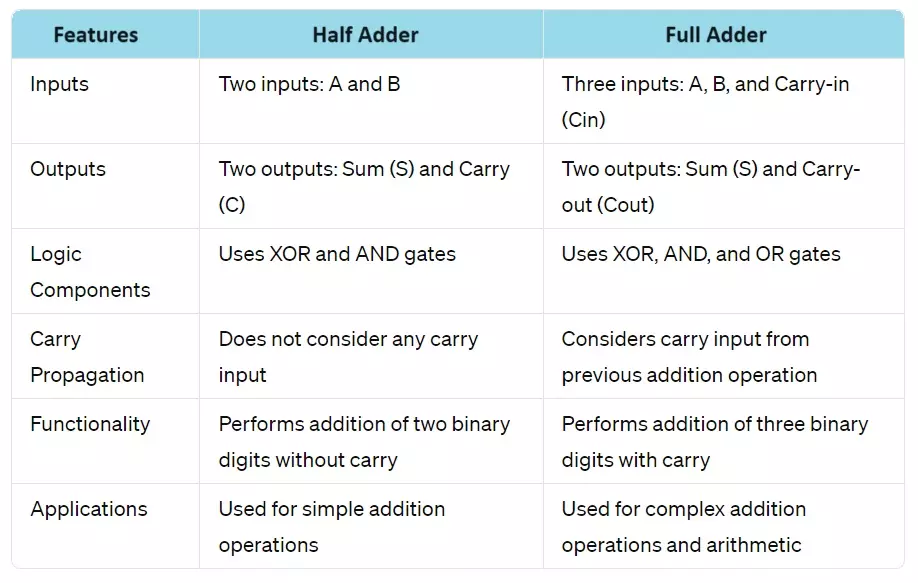
In summary, while both half adders and full adders perform binary addition, from half and Full adder truth table the key distinction is that a full adder can incorporate a carry input from previous addition stages, enabling it to add multi-bit binary numbers, whereas a half adder cannot handle such carry inputs.
4 Bit Adder Circuit using IC 7483:
One commonly used integrated circuit (IC) for implementing a full adder is the 74LS283, which is a 4-bit binary full adder. This IC contains four independent full adder circuits within it, allowing it to perform addition on four sets of binary inputs simultaneously.
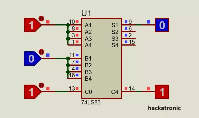
Here are some key features of the 74LS283 IC:
- It operates on a single power supply voltage typically in the range of 4.75V to 5.25V.
- It has four full adder circuits, each capable of adding three binary inputs.
- The outputs of each full adder are available individually (sum and carry out).
- It typically comes in a 16-pin DIP (Dual In-line Package) form factor.
You can refer to the datasheet of the 74LS283 IC for detailed pinout information, electrical characteristics, and application circuit examples.
The CD4008 is another 4-bit adder IC based on CMOS (Complementary Metal-Oxide-Semiconductor) which is commonly used in digital circuitry. It is designed to perform arithmetic operations on binary numbers. Here’s some information about the CD4008 IC:
- It typically operates with a supply voltage (VDD) ranging from 3 volts to 18 volts.
- It can perform addition operations on two 4-bit binary numbers, producing a 4-bit sum output and a carry-out bit. Also having a carry input pin for carry in.
Keep in mind that there are many other full adder ICs available from different manufacturers, each with its own set of features and specifications. The choice of IC depends on the specific requirements of your application.
Universal NOR Gate Truth Table, Logic Circuit and IC PIN Diagram
Applications of Half adder and Full adder:
Half adders and full adders are fundamental building blocks in digital electronics, and they find applications in various fields.
Half Adder:
- Binary Addition: The primary application of a half adder is in binary addition. It adds two single-bit binary numbers and produces their sum and carry output.
- Address Calculation: In computer architecture, half adders are used in address calculation units to calculate memory addresses.
- Logic Circuit Design: Half adders are often used as basic building blocks in the design of more complex digital logic circuits.
Full Adder:
- Binary Addition: Full adders are used to perform addition of multi-bit binary numbers. They can add two binary digits along with a carry input, producing their sum and carry output.
- Arithmetic Logic Units (ALUs): Full adders are essential components of ALUs, which are the core processing units in CPUs (Central Processing Units). ALUs perform arithmetic and logic operations on binary numbers, and full adders are used to add two binary numbers together.
- Digital Signal Processing (DSP): In DSP applications, full adders are used in the implementation of various algorithms such as filters, transforms, and signal processing operations.
- Multiplexers and Demultiplexers: Full adders can be used in the design of multiplexers and demultiplexers, which are used in data communication systems for routing and selecting data.
- Counter Circuits: Full adders can be used in the design of counter circuits, which are used to count events or pulses in digital systems.
- Parallel Adder/Subtractor: Full adders can be used in parallel adder/subtractor circuits, which can perform addition or subtraction of multi-bit binary numbers.
- Error Detection and Correction: Full adders can be used in error detection and correction circuits, such as parity generators/checkers, which are used to detect and correct errors in data transmission.
What is Flip Flop Circuit? Types of Flip Flops with Truth Table

Beautiful tutorials here on hackatronic !! However, i think your full adder diagram has mistakes. For the final carry, the two carry are inputs to an OR gate, not XOR.
I have updated the table. You can check it.
Thank you