This article explains an H-Bridge inverter circuit based on the SG3525 IC and MOSFETs like IRFZ44N or IRF3205 or IGBT like GT50JR22, which can convert DC to AC with a frequency of 50Hz or 60Hz, suitable for most standard applications. The SG3525 is a widely used PWM (Pulse Width Modulation) controller IC designed for various power electronics applications, including DC to AC inverters.
H-Bridge Inverter Circuit Overview
The SG3525-based H-Bridge inverter circuit converts low-voltage DC into high-voltage AC, making it ideal for use in applications like renewable energy systems, backup power supplies, and portable inverters. Below is a detailed description of the circuit components and their roles. You can also see block diagram of SPWM inverter circuit.
Components Required
- SG3525A PWM Controller IC
- N-channel MOSFETs (IRFZ44N or IGBT)
- Step-up Transformer (12V to 230V based on desired AC output voltage)
- Capacitors and Resistors (For filtering and frequency tuning)
- Diodes (1N4728A Zener diode and 1N4148 for protection)
- Inductors (Optional for output filtering)
- Power Supply (e.g., a 12V DC battery)
SG3525A IC Pinout Configuration
The SG3525 is a powerful PWM controller IC designed for efficient energy conversion. It offers features like an internal oscillator, soft start, under-voltage lockout, and shutdown capabilities. Here’s an overview of its pin functions:
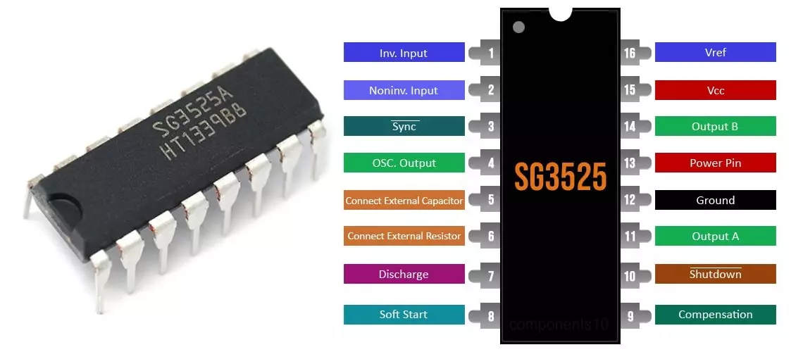
- Pin 1 (INV): Inverting input of the error amplifier, typically connected to the feedback signal.
- Pin 2 (NI): Non-inverting input of the error amplifier, often tied to a reference voltage.
- Pin 3 (SYNC): Synchronization pin for external clock inputs.
- Pin 4 (OSC): Pin for connecting the timing capacitor, used to set the oscillator frequency.
- Pin 5 (CT): Timing capacitor pin for controlling the internal oscillator frequency.
- Pin 6 (RT): Timing resistor pin for oscillator frequency adjustment.
- Pin 7 (DISCHARGE): Discharges the timing capacitor during each oscillator cycle.
- Pin 8 (SOFT-START): Controls the startup process with a capacitor to ensure a gradual increase in output.
- Pin 9 (COMP): For feedback loop stability and compensation.
- Pin 10 (SHUTDOWN): Activates the shutdown feature to disable the output stages immediately.
- Pins 11 & 14 (OUT A, OUT B): PWM outputs to drive external MOSFETs.
- Pin 12 (VCC): Main supply voltage input.
- Pin 13 (GND): Ground connection.
- Pin 15 (VC): Supply voltage for the output stage.
- Pin 16 (VREF): Provides a 5V reference for external components.
Setting the PWM Frequency
The PWM frequency of the SG3525 is determined by external timing components resistors and capacitor (RT and CT) connected to Pins 5 and 6. The following formula calculates the oscillator frequency:
F = 1 / (CT × (0.7 RT + 3 RD))
Where:
- F = Frequency in Hz
- CT = Timing Capacitor (F)
- RT = Timing Resistor (Ω)
- RD = Deadtime Resistor between pins 5 & 7 (Ω)
For example, with the following component values:
- CT = 1µF
- RT = 14kΩ
- RD = 47Ω
Substituting these into the formula:
F = 1 / (1 × 10⁻⁶ × (0.7 × 14 × 10³ + 3 × 47))
F ≈ 100.59Hz
This frequency can be adjusted depending on the application requirements, such as 50Hz or 60Hz for AC power output.
Designing The H-Bridge Inverter Circuit Using IC SG3525
The SG3525 IC when combined with an H-bridge configuration of complementary MOSFETs, becomes an efficient solution for converting DC voltage to AC power. With the integration of additional components for output voltage regulation and low battery cut-off, the circuit can ensure reliable performance and protection for connected devices.
Key Components of H-Bridge Inverter Circuit
The H-bridge inverter circuit comprises several critical components, each contributing to the efficient operation of the system. Below is an overview of the primary elements:
- SG3525 IC: The main controller for generating PWM signals to drive the MOSFETs in the H-bridge configuration.
- H-Bridge MOSFETs: Power transistors (typically N-channel MOSFETs such as IRFZ44N or IRF3205) that switch the DC voltage to generate an alternating waveform.
- Driver Circuit: Interfaces the SG3525 with the MOSFETs to ensure proper switching.
- Step-Up Transformer: Converts the low-voltage DC input into higher-voltage AC output.
- Voltage Feedback Circuit: Ensures output voltage regulation by adjusting the PWM duty cycle.
- Low Battery Cut-Off Circuit: Disconnects the load when the battery voltage falls below a safe threshold, protecting the battery from over-discharge.
- Protection Circuits: Provides safeguards against overcurrent, overheating, and short circuits (optional).
- Low-Pass Filter: Converts the PWM signal into a smoother AC waveform for sensitive devices (optional).
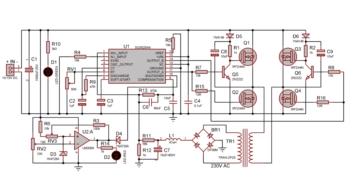
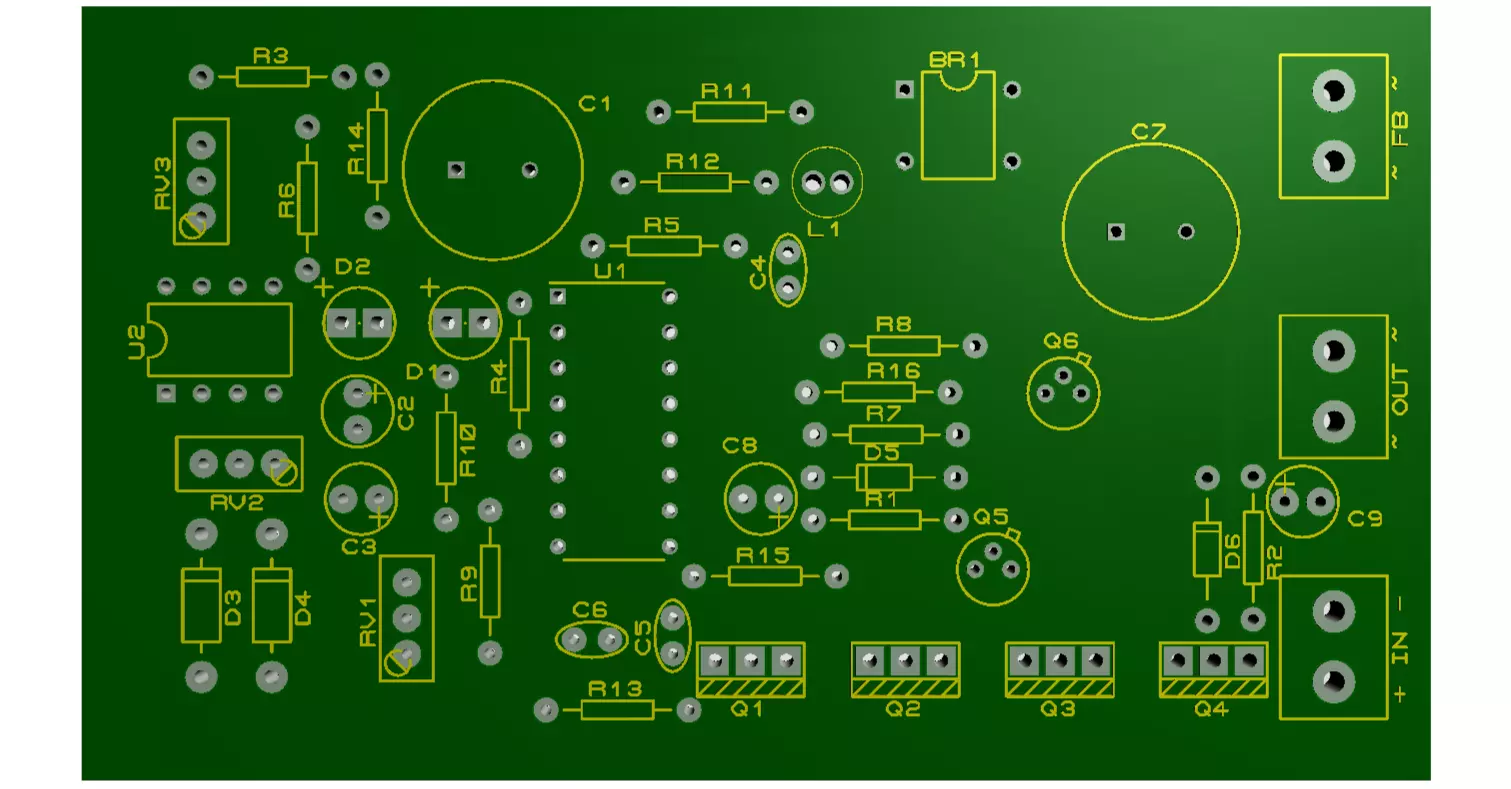
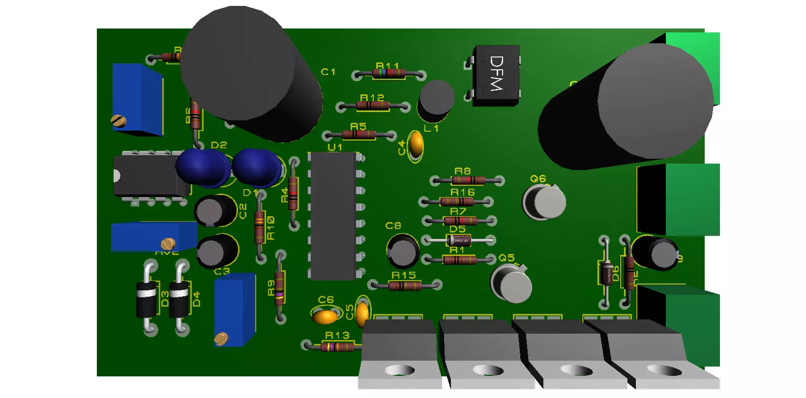
SG3525 Based H Bridge Inverter Circuit Schematic
Below is the schematic description of the SG3525 based H-bridge inverter circuit:

Component List
- Resistors:
- R1, R2 = 1kΩ
- R3 = 100kΩ
- R4, R5, R6, R7, R8 = 10kΩ
- R9 = 47Ω
- R10 = 3.3kΩ
- R11 = 56kΩ
- R12, R14 = 1kΩ
- R13 = 470kΩ
- R15, R16 = 10Ω
- RV1 = 50kΩ preset
- RV2, RV3 = 10kΩ presets
- Capacitors:
- C1 = 1000µF/25V
- C2, C3 = 1µF
- C4 = 0.1µF
- C5 = 10nF
- C6 = 68nF
- C7 = 10µF/450V
- C8, C9 = 10uF
- Inductor: L1 = 47µH
- Diodes:
- D1 = Green LED
- D2 = Red LED
- D3, D4 = 1N4728A Zener
- D5, D6 = 1N4148
- Transistors and ICs:
- Q1, Q2, Q3, Q4 = IRFZ44N MOSFETs
- Q5, Q6 = 2N2222
- U1 = SG3525A IC
- U2 = LM358 or LM393
- Other Components:
- 12V to 220V step up transformer
- 12V battery
- Screw terminals (2, 2, 2)
Detailed Working of SG3525 H Bridge Inverter Circuit
1. SG3525 PWM Controller
The SG3525 IC serves as the core of the circuit, generating complementary PWM signals for driving the MOSFETs in the H-bridge configuration.
- Pin 1 (INV) and Pin 2 (NI): These inputs are used for feedback control to regulate the output voltage. A voltage divider circuit from the output provides a feedback signal to the error amplifier, which adjusts the PWM duty cycle.
- Pin 5 (Oscillator Timing Capacitor): A capacitor connected here determines the oscillator frequency, typically set for a 50 Hz AC output.
- Pin 6 (Oscillator Timing Resistor): Works with the timing capacitor to set the frequency.
- Pin 8 (Soft Start): A capacitor connected to this pin controls the gradual ramp-up of PWM signals, reducing the risk of inrush current.
- Pin 9 (COMP): This pin allows loop stability through compensation.
- Pin 10 (Shutdown): Used for disabling the PWM outputs when the low battery cut-off is activated.
- Pins 11 and 14 (Outputs A & B): Provide complementary PWM signals to drive the gates of the MOSFETs.
2. H-Bridge MOSFET Power Stage
The H-bridge stage consists of four N-channel MOSFETs (e.g., IRFZ44N), which switch the DC voltage across the transformer’s primary winding to generate an alternating waveform.
- Gate Resistors: Resistors are connected to the MOSFET gates to limit the gate charging current and prevent ringing.
- Flyback Diodes: Diodes across the MOSFETs protect them from voltage spikes caused by the inductive nature of the transformer.
3. Step-Up Transformer
A 12V to 230V step-up transformer is used to convert the low-voltage DC input (typically 12V to 15V) into high-voltage AC output (220V to 240V). The turns ratio of the transformer must match the desired output voltage.
- The MOSFETs drive the transformer’s primary winding, and the secondary winding delivers the required AC output.
- Connect the 12V battery to the input terminal and the transformer’s primary terminals to the H-bridge’s output terminals.
4. Output Voltage Regulation
Voltage regulation is achieved using a feedback circuit. A voltage divider network on the transformer’s secondary (AC output) reduces the output voltage to a suitable level for the SG3525’s feedback input. This feedback signal is fed to the error amplifier (Pin 1), allowing the IC to adjust the PWM duty cycle and maintain a stable output voltage.
5. Low Battery Cut-Off Circuit
A low battery cut-off circuit protects the battery from over-discharge.
- Voltage Divider for Monitoring: A resistor divider reduces the battery voltage for comparison.
- Comparator Circuit: An operational amplifier (e.g., LM358 or LM393) monitors the battery voltage. When the voltage drops below a preset threshold (e.g., 10.5V for a 12V battery), the comparator pulls the SG3525’s shutdown pin (Pin 10) high, disabling the PWM outputs.
- Zener Diode: 1N4728A diode provides a stable reference voltage for comparison and protects the IC.
6. Optional Features
- Low-Pass Filter: To smooth the PWM waveform into a sinusoidal shape, an LC filter (inductor and capacitor) can be added to the circuit. This is particularly useful for sensitive devices requiring pure sine wave output.
- Protection Circuits: Overcurrent protection and short-circuit protection can be added to safeguard the MOSFETs and other components.
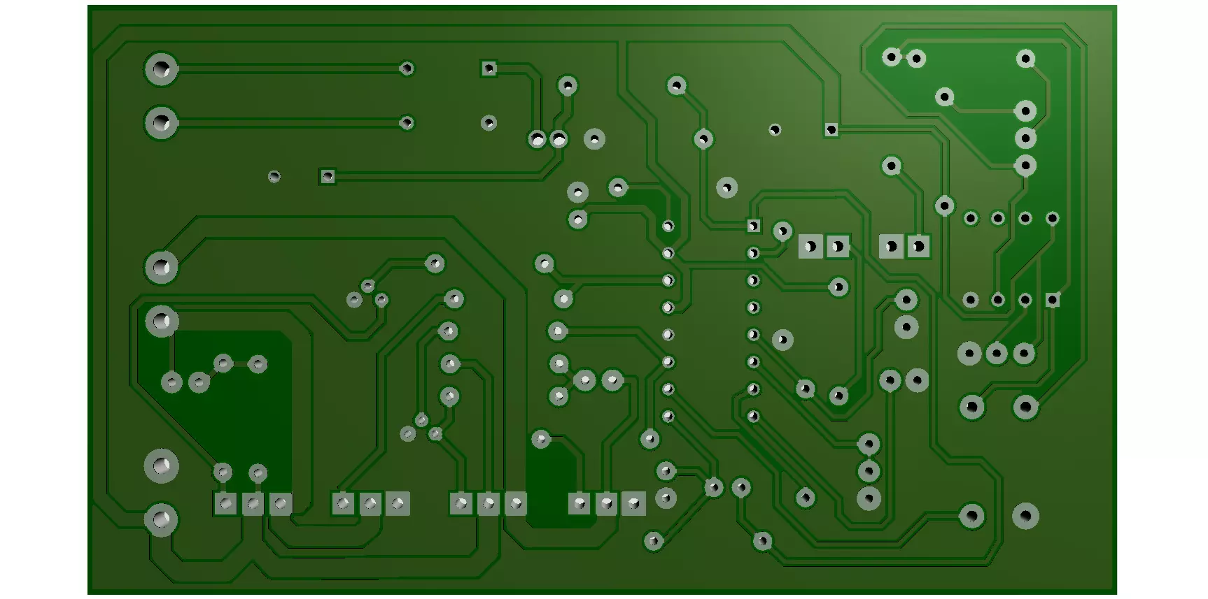
PCB Design and Assembly
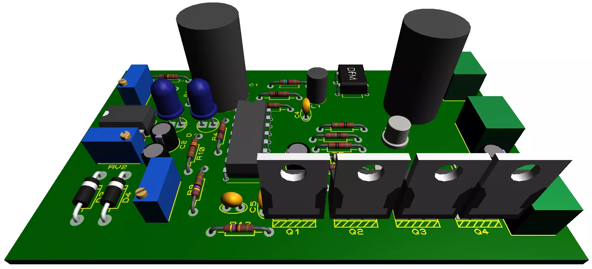
PCB Layout
The inverter circuit can be implemented on a PCB with thick copper traces to handle high current. Soldering the tracks can further enhance current-carrying capacity.
Connections
- Connect the transformer output to the feedback input terminal.
- Ensure proper heat dissipation for the MOSFETs by attaching heatsinks to manage thermal performance.
Considerations for Reliable Operation
- Feedback Accuracy: Ensure precise feedback for stable voltage regulation and consistent output frequency.
- Thermal Management: Use adequate heatsinks for the MOSFETs to prevent overheating during operation.
- Component Ratings: Select components with appropriate voltage and current ratings to match the load requirements.
- Testing: Before connecting a load, test the circuit thoroughly to ensure proper operation and safety.
Conclusion
The SG3525-based H-bridge inverter circuit is a reliable and efficient solution for converting DC voltage to AC power. With features such as voltage regulation and low battery protection, it is suitable for powering a wide range of devices. By incorporating additional modifications, such as an SPWM generator or low-pass filters, the circuit can produce pure sine wave outputs, making it ideal for sensitive appliances. This circuit is an excellent choice for various inverter applications, from basic setups to advanced systems requiring enhanced functionality and safety features.
Star Delta Connection in Three Phase Power Systems
Switch Mode Power Supply SMPS Block Diagram & Working
12V to 230V Inverter Circuit Diagram using 555 timer IC

Good job,thanks for sharing your knowledge. Please is transformer a center tap or two wire transformer?
It’s a two wire transformer
Is it a modified sine wave?
NO, Square Wave
Can. Use UPS transformer?
What watt is the circuit?
Good for 0.5KW
What’s is the vin for sg3525
Should I use a voltage regulator?
If yes , what volt?
From 8V to 35V no need of voltage regulator.
Hello brother,
what do transistors Q5 and Q6 do in the circuit?
Is the SG IC capable of driving more MOSFETs?
Thank you for your answer.
Transistor Q5 and Q6 are used to Drive the MOSFETs
you can connect more MOSFETs for more current.
Hello brother
the SG IC has a power output of 400 mA
why is a transistor used for driving?
Thank you for your answer.
Complementary Switching
Hello and thank you, Mr. Engineer,
for a 180-degree phase difference in the outputs, the MOSFETs can be set up in a cross-connection, meaning the gates of the MOSFETs Q1 and Q4 are connected together, and the gates of the MOSFETs Q2 and Q3 are connected together.
What is your opinion, dear friend?
Thank you for your quick response 🙏
OK, do it and see the outcome!
Thank you for your guidance.
sir please how can I use three in center tap t
ransformer
Use this circuit
SG3525 PWM Inverter Circuit
ok thank you sir
Hi, I apologize if this may be a silly question, but I can’t figure out why I have to program the oscillator to 100Hz to get 50Hz. How can the circuit output 50Hz if the oscillator operates at 100Hz? Can you explain? Thank you so much.
The SG3525 has an internal flip-flop that splits the oscillator frequency in half. So, if you want a 50Hz output, the oscillator needs to run at 100Hz. That way, the chip switches between its two outputs 100 times per second, giving you 50 full cycles (positive and negative) per second — which equals 50Hz AC.
Hi, I don’t know how to thank you because finally someone was able to give me a simple yet precise explanation.
So, specifically, if I used the following values: 1uF for CT, 12K+2K for RT, and 47 Ω for RD, could I get 100 Hz oscillator and a 50 Hz output?
Thank you very much, and a big handshake.
Hi, would it be possible to purchase the PCBs?
Thank and a greeting.
Visit PCBWay
Hi, I noticed that in the component list you indicated: U2 = LM358 or LM393. Is there a mistake? Because the two ICs are not compatible. The LM358 is an op amp while the LM393 is a comparator. They are pin-to-pin but completely different. How is this possible? Thank.
You can use LM358 but it’s not a good choice for this circuit, instead of this you should use LM393 which is a good comparator and connect it 5V Vref Pin 16.
Okay, thanks for the reply.
But your answer isn’t exhaustive, and the problem remains. I had your PCBs made, which are designed to accommodate the 358, since I hadn’t immediately noticed the strange contradiction of U2.
Now I ask you:
if you already knew that the LM358 wasn’t a good choice for the circuit, why did you design the PCB for the LM358 and not the LM393? And now how can I use the 5 PCBs already made if they’re not compatible with the LM393?
Waiting your kind reply. A greetings.
Have you assembled and tested the PCB?
No, I bought the components and had the PCBs made, but then I noticed the oddities with U2 and didn’t assemble the project. I’d like to know which IC to use. What do you think?
Continue with LM358 and see the results, how it performs?
You can also check it with and without LM358 section in the end.
But using an OpAmp as a comparator isn’t a good solution. That circuit violates the LM358’s common-mode specifications. I should use an LM393, but I don’t think it will work on your PCB, including the components orbiting it…
Even superficial tests are self-defeating; they waste components.
But what I don’t understand is: if you knew the LM393 was needed, why did you specify an LM358? The PCB that matches your Gerbers and that I had made is useless and should be discarded…
Waiting for your kind reply. A Greeting.
One thing you should do is change 1N4728A to 1N4732A or 1N4733A for better protection of shutdown pin 10.
You can also edit the proteus file, change this LM358 circuit to LM393 and share your work with us so we can get a better understanding of how both perform?
Can you specify in detail what you mean by the LM393, “connect it to the 5V Vref pin 16.”? If you can help me understand, I’ll run the tests and then report back to the thread. Thank and a greeting.
Yes, connect LM393 to the 5V Vref pin 16 and then set the threshold for checking.
Share your observations here…
Hi, I find the project interesting, although I’m a bit skeptical about some of the resistive components and think they deserve further testing. I’ll certainly share my observations and implementations here, but I need more detailed answers. It’s not enough to simply say, “Connect the LM393 to pin 16 of the 5V Vref and then set the control threshold.” Do you mean power pin 8 or non-inverting pin 3? And if it were pin 3, do you think it should be connected directly to pin 16 without a limiting resistor? Then the hysteresis control circuit would be significantly different, and without a limiting resistor, the hysteresis adjustment could also directly affect pin 16, which wouldn’t be a wise choice. Unfortunately, I’m not familiar with the LM393 (I’ve never used it), and if you have more knowledge of the component, it would be helpful to get more direct help from you. Thank.
All you have to make is a comparator circuit!
Powering LM393 IC:
LM393 pin 8 → +5 V (use a separate 5V supply like LM7805)
LM393 pin 4 → GND
Making Adjustable Battery Sense:
Connect Pin 3 − → fixed 5 V reference (from SG3525 pin16)
Wiper (middle) of the pot → LM393 inverting input (pin 2).
Connect Battery + → left leg of the 100 kΩ pot.
Connect right leg of the 100 kΩ pot → the 24 kΩ resistor → then to Battery GND.
Keep the pull-up on the LM393 output (10 kΩ to +5 V).
Adding Hysteresis:
Add Rfb (50k to 100k) between LM393 pin 1 (output) and LM393 inverting input (pin 2).
Do not connect Rfb to SG3525 pin16 (VREF).
I’m sharing this here, but you shouldn’t delete the posts…
Keep in mind that I have the Multisim simulator, not Proteus, but both Proteus and Multisim don’t have the SG3525 controller, so I can only simulate the sections of the schematic that can be simulated without the SG3525.
You can find SG3525 in Proteus 8
I have Proteus Pro 8.8 SP1, but the SG3525 integrated circuit is missing. I’ve searched extensively online but haven’t found the component for Proteus.
The SG3525 isn’t available (even) with Multisim, nor can it be created with Spice, as this component is officially declared incompatible with Multisim version 14.3, and I have that version.
Regarding the low battery detection circuit, I’ve already built it with an LM393, but I couldn’t connect it to the SG3525 because the SG3525 doesn’t exist in the simulator and I couldn’t simulate it. In any case, I’d prefer not to risk overloading the SG3525, thus also minimizing any interference. In practice, I preferred to stabilize the entire low battery detection circuit with an LM78L05 and draw only the portion for comparison from the 12V using a divider. It works well, and I’ve even included an SCR to prevent the device from automatically restarting after shutdown. When the battery reaches low charge, the best thing to do is to lock the inverter so that it restarts only with external intervention from the operator, for example, when the battery is recharged.
This is because, when the inverter shuts down, the battery voltage automatically rises again, so be careful to manage the situation wisely to avoid constant STARTS and STOPS, which are not advisable.
I note that the SG3525 datasheet lists recommended values for the oscillator capacitor [Pin 5 (CT)] as between 0.001 and 0.2uF. You are using 1uF (five times larger), and an electrolytic capacitor, which is certainly not ideal for this application.
Furthermore, your website doesn’t allow for the publication of electrical diagrams, so I imagine that the sharing you requested is limited to some theoretical and concise descriptions of the work progress.
I am happy to see that you are finding important errors it this circuit.
I will suggest you use a 0.1uF capacitor with 200kΩ potentiometer.
Using SCR is a good idea to stop the circuit.
If you don’t have SG3525 IC, then try to find any similar IC.
You can mail me your circuits, also you can connect with me on WhatsApp.
I forgot one detail: The voltage across a battery when it powers an inverter is very “dirty”—excuse me for this non-technical term—so it’s necessary to filter your reading.
You should use filter capacitors to eliminate this issue.
Are you working on physical PCB?
I’m making some corrections, but I’m short on time and my work is progressing slowly, and I occasionally forget something. As for the capacitor, I can easily use a 1uF capacitor, but I’d avoid electrolytics. However, I think it would be better to achieve 100Hz from the oscillator within the manufacturer’s recommended range, that is, by reducing the capacitive value and compensating with the resistive value.
Using an SCR is essential for the reasons already mentioned.
I can’t use a component other than the SG3525 because I bought 20 of them, like a megalomaniac, and now I have to proceed with that. Unfortunately, there’s no way to simulate it. The software component is missing.
My schematics are only sketches and not final. I could send them to you, but I haven’t found your contact information.
I agree about the filter capacitors, but perhaps an inductor will also be needed, but I need to find the value first because I imagine it will be huge for 500W…
Furthermore, I’m not working on a physical PCB but on the Multisim 14.3 simulator.
Obviously, since I can’t fit the SG3525 into the simulator, I’m forced to work on separate sections.
I also added a draft of an input power regulator using an ACS758-50 Hall sensor, but, again, it’s only a draft at the moment.
Try installing older versions of proteus like proteus 8.1 it has SG3525.
If you have 20 pieces of SG3525 then you should test in on breadboard.
You can find my contact details on contact us page and social media.
I installed Proteus 8.1 Pro SP1 but the SG3525 is missing…
I have Proteus 8.12 SP0 it has SG3525.
Yes, in version 8.12 there’s a UC3525A that I believe is equivalent, but that version is not very usable. It contains few components, and they’re all SMD. It’s probably inactive or there are missing libraries…
How is your progress on this circuit, are you building it physically?
No, I’ve only tested separate sections on a breadboard, but first I’d like to try to solve a 12V input power limiter, but I haven’t gotten any good results yet. Before fully building the device, I’d prefer to simulate it, but the challenge is finding a simulator that has all the necessary components.
Ok, keep updating us about this circuit.
But can you tell me why there are only SMD components in version 8.12 of Proteus? Are there any libraries I should add? I don’t know where to find them…
One thing you can do is, run your simulation in Proteus and make your final PCB from EasyEDA.
Yes, but I need the Proteus component libraries. Where can I find them?
Which library?
I need the libraries for all Proteus discrete components. It’s impossible for version 8.12 to contain only SMD components, and even then only a few. If anyone knows where to find them, please let me know; otherwise, I can’t simulate. Thank.
it’s not working, can you give the working file plz….
I have given all the files you can edit it by yourself.
But isn’t the voltage coming out of R11 too high? 22.5V…
It should be around 5.7V
Yes and no. I used a calculator on the web to confirm the voltage of the feedback section at pin1 of the SG3525 and it is about 4V.
Yes, your assessment is correct, but I would add a trimmer to the R11/R12 feedback divider, for possible tolerances.
Then I would ask you if you could kindly email me the Proteus source file, so I don’t have to retrace everything. I would need to add all my implementations to that file, then I’ll send you the complete source. I’ve created some SCR interrupts, crowbar-style, and added an input power regulator with a Hall sensor, but my format isn’t compatible with Proteus and I can’t simulate it.
You can download the Proteus source file at the end of article.
Thank, I hadn’t seen that. I downloaded it, but it doesn’t work with the simulator. It seems that the UC3525A is connected incorrectly or the pins do not match the original, so, it is not possible to simulate it.
Here are the error messages:
No model specified for U1. [U1]
Simulation FAILED due to partition analysis error(s).
There were more, but I fixed them, but the one for U1 is a problem. It almost requires rebuilding the schema.
Yes, it is not possible to simulate this one (I have same problem).
That’s why i was saying to test it on breadboard.
I have not found any simulation model for SG3525.
I used the UC3525A, which is identical to the SG3525. I built my entire project with that IC, but the simulator gives me simulator setup errors. Maybe the schematic is too large for the simulator’s default, but I don’t know what I need to adjust.
I’ll send you the simulator log messages. Maybe you know what to change. I’m familiar with Multisim, but I’ve never used Proteus and I’m not familiar with it.
Message Proteus
PROSPICE 8.08.00 (Build 29194) (C) Labcenter Electronics 1993-2021.
Loaded netlist ‘C:\Users\Maxbi\AppData\Local\Temp\LISA3921.SDF’ for design ‘MIO UC3525A Pwm Controller FULL BRIDGE.pdsprj’
[SPICE] Gmin step [0 of 120] failed: GMIN=0.001
[SPICE] Gmin stepping failed
[SPICE] transient GMIN stepping at time=3.125e-009
[SPICE] transient GMIN stepping at time=3.125e-009
[SPICE] TRAN: Timestep too small; timestep = 1.25e-019: trouble with node #00030.
What is node #00030?
well i don’t have much idea.
Add a high-value resistor from suspicious nodes to ground (e.g., 1MΩ). This cures floating nodes.
No, Proteus isn’t a serious simulator. I’m not familiar with it, and it’s incomprehensible to me. I can’t simulate it. It keeps throwing up errors that don’t make sense. Unfortunately, Multisim is missing some components otherwise, I would have solved the problem by now. I think that even though I’ve completed the schematic, I’ll have to abandon the project.
As you wish
Do you have any other option/project?
No, I don’t have anything else. Unless I find a simulator that can simulate the project.
So, you don’t want it on breadboard or PCB before simulation!
Well, I’ve gotten used to simulating before building. If you want, I can email you the complete source code. If you want to make the PCB yourself, you know Proteus… I don’t know Proteus, and it’s already pissed me off enough with its absurd errors…
Not interested!
It’s a shame, it’s fully equipped and has been tested in separate and independent areas, but never as a whole. It will remain an idea that has never been fully tested. Best regards…
See this simulation https://everycircuit.com/circuit/5908847876898816/sg3525-pwm-h-bridge—copy
You should consider a breadboard trial as you have all the components.
Rest is your choice…
Also, you can mail me your work till now.
Yes, I saw it, but what I saw is only a part, and the simplest one at that. Mine, on the other hand, is complete. The source code is missing some protection and noise suppression components because the simulator doesn’t have them, but I included them in the FidoCadj schematic. I tested the circuit on a breadboard with separate blocks because the breadboard didn’t fit everything, but every single block worked properly.
My circuit includes a real low battery monitor and an input power regulator that can be manually set as if it were a linear PSU.
Maybe in the future I’ll be able to simulate it. I’m not one to give up easily. A greeting.
Amazing!