Let’s see IC OP AMP IC 741 Pin Diagram and working with its applications operational amplifier IC 741 is one of the oldest and most popular IC with high performance.
It’s been around since the 1960s and is still used in various applications today. The “741” refers to the model number assigned by the manufacturer, Texas Instruments.
It is used in various analog applications such as adder integrator and differentiator summing amplifier etc.
An operational amplifier is a DC-coupled high-gain electronic voltage amplifier that has high gain, differential input, high input resistance, and low output resistance.
IC LM741 OP AMP
Advantages/Special Features of IC 741 OP AMP:
General Purpose: The 741 is a general-purpose op-amp suitable for a wide range of applications in analog electronic circuits.
Single Operational Amplifier: The IC 741 contains a single operational amplifier in an 8-pin dual in-line package (DIP).
Low Input Offset Voltage: The 741 typically has a low input offset voltage, meaning that the output voltage is close to zero when the input voltages are equal. It has offset voltage null capability.
High Input Impedance: The input impedance of the 741 is high, which means it draws very little current from the input source.
High Gain: The 741 has a Large differential voltage gain, typically around 100,000 or more.
Wide Frequency Response: It has a wide frequency response, typically from a few hertz to several megahertz. Frequency compensation is not required.
Low Input Bias Current: The 741 has low input bias current, which reduces errors in applications where input currents are significant.
Short Circuit Protection: It usually incorporates short-circuit protection, safeguarding the device from damage in case of output short circuits.
Operating Voltage: The typical operating voltage for the 741 is between ±5V and ±18V.
Temperature Range: It can operate over a wide temperature range, typically from -55°C to 125°C, making it suitable for various environments.
Low Cost: One of the advantages of the 741 is its low cost, making it accessible for a wide range of applications.
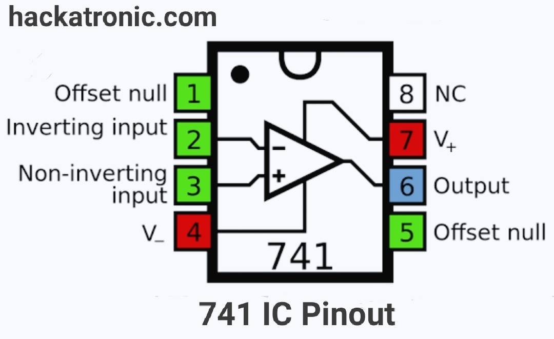
OP AMP IC 741 Pin Diagram/Pinout:
OP AMP IC 741 Pin Diagram
The operational amplifier (op-amp) IC 741 is a widely used integrated circuit in electronics. It has eight pins, each serving a specific purpose:
Offset Null (NC): This pin is usually not connected (NC). It was used in older versions of the 741 op-amp for offset nulling, but modern versions typically don’t utilize it.
Inverting Input (-): This pin is denoted with a negative (-) sign and is used as the inverting input terminal of the op-amp.
Non-Inverting Input (+): This pin is denoted with a positive (+) sign and is used as the non-inverting input terminal of the op-amp.
V- (Negative Power Supply): This pin is connected to the negative power supply terminal.
Offset Null (NC): Similar to pin 1, this pin is usually not connected (NC) in modern applications.
Output: This pin is the output terminal of the op-amp.
V+ (Positive Power Supply): This pin is connected to the positive power supply terminal.
NC: This pin is typically not connected and left unused.
This is standard OP AMP IC 741 Pin Diagram but do check the datasheet of the specific manufacturer for any variations or additional features. OP AMP IC 741 is available in many other packages.
Important characteristics of IC 741 op-amp:
Sr, No
Characteristics
Value for IC 741
Ideal value
1
Input resistance Ri
2M ohm
infinity
2
Output resistance Ro
75 ohm
0
3
Voltage gain Av
2*10^5
infinity
4
Bandwidth B.W.
1MHz
infinity
5
CMRR
90dB
infinity
6
Slew rate S
0.5V/uS
infinity
7
Input offset voltage Vios
2mV
0
8
PSRR
150uV/V
0
9
Input bias current Ib
50nA
0
10
Input offset current
6nA
0
Working of IC 741 Op-Amp:
IC 741 is widely used operational amplifiers (Op-Amps) in various electronic circuits due to its versatility and reliability. Here’s a brief overview of its working:
Internal Circuitry: The IC 741 contains multiple transistors, resistors, and other components integrated into a single chip. Its internal circuitry consists of several stages, including differential amplifier stage, gain stage, output stage, and compensation network.
Differential Amplifier Stage: The input stage of the 741 consists of a differential amplifier. This stage amplifies the voltage difference between its two input terminals (inverting and non-inverting). The gain of this stage is typically very high, providing high input impedance and low output impedance.
Gain Stage: The amplified voltage from the input stage is then further amplified by the gain stage. The 741 has a high open-loop voltage gain, typically around 100,000. This gain can be adjusted using external feedback components like resistors.
Output Stage: The output stage of the 741 is designed to provide a high output current capability while maintaining a low output impedance. It also ensures compatibility with various loads.
Compensation Network: The 741 incorporates internal compensation to stabilize its operation and prevent oscillations. This compensation network typically consists of capacitors and resistors.
Power Supply: The IC 741 requires dual power supplies (positive and negative) for its operation. These power supplies typically range from ±5V to ±15V.
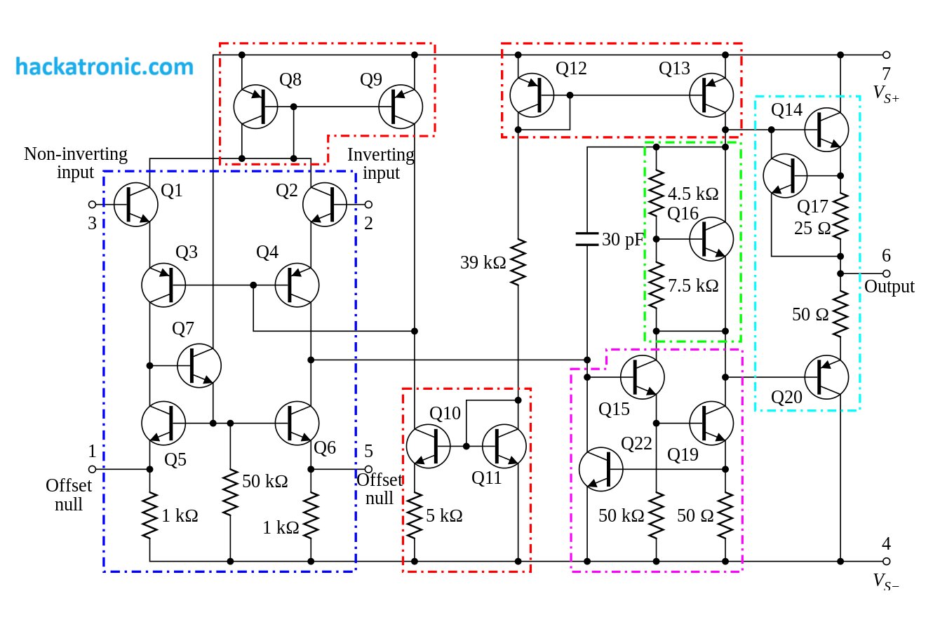
IC 741 Op Amp Transistor Level Circuit
Internal Circuit of IC 741 Operational Amplifier:
The internal circuitry of the IC 741 operational amplifier. Let me summarize the key points based on your description:
Input Stage with Transistors Q1 and Q2: These transistors serve as the input stage of the op-amp, with Q1 connected to the inverting terminal and Q2 connected to the non-inverting terminal. This configuration helps to isolate the input signals and prevent feedback.
Current Mirrors (Q8/Q9 and Q12/Q13): These circuits regulate the current flow within the op-amp, ensuring stable operation and minimizing the impact of input voltage fluctuations on internal circuitry.
Voltage Level Shifter (Q16): This circuit reduces the voltage level from the amplifier circuit at the input section before passing it to the next stage. This helps prevent signal distortion.
Class A Amplifier Stage (Q15, Q19, Q22)andOutput Stage (Q14, Q17, Q20): These stages are responsible for amplifying the input signal and driving the output with sufficient power. The class A amplifier stage ensures linear amplification with minimal distortion.
Offset Null Configuration (Q5, Q6, Q7): These transistors are part of a configuration that allows for offset null adjustment, balancing both the inverting and non-inverting inputs to minimize any irregularities at the input phase of the differential circuit.
Overall, these components and circuits work together to ensure the proper operation of the IC 741 op-amp, providing high gain and stable amplification for various applications.
Mode of operation:
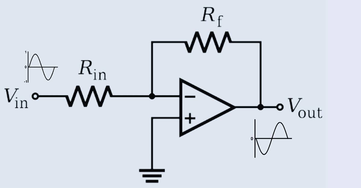
The 741 can operate in both inverting and non-inverting configurations. Inverting configuration means the output is inverted concerning the input signal, while non-inverting configuration maintains the same phase.
By connecting the input signal to the inverting terminal (-) and providing feedback from the output to the inverting input, the op-amp can be configured to produce an inverted and amplified output signal relative to the input.
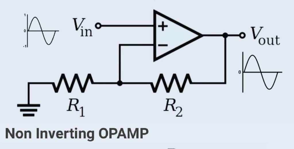
Here, the input signal is connected to the non-inverting terminal (+) and feedback is applied from the output to the inverting input. This configuration produces a non-inverted and amplified output signal relative to the input.
Gain (Av) = 1 + (R2/R1)
741 IC is used in various modes.
As a buffer Amplifiers
Summing Amplifier
Difference Amplifier
Schmitt trigger
Integrator
Comparator
IC 741 Op-Amp Applications:
The IC 741 finds applications in various circuits such as amplifiers, filters, oscillators, voltage followers, comparators, and many more.
Log and Antilog Amplifier:
The IC 741 op-amp can be used to create log and antilog amplifiers. These circuits are essential for mathematical operations and signal processing.
Amplifier:
As a general-purpose amplifier, the 741 op-amp can amplify weak signals. It’s commonly used in audio amplification, instrumentation, and other applications where signal gain is necessary.
Voltage Comparator:
The 741 op-amp can compare two input voltages and provide a high or low output based on their relative magnitudes. This functionality is useful in threshold detection and switching applications.
Active Filter:
By configuring external components like capacitors and resistors, the 741 op-amp can function as an active filter. It’s commonly used in low-pass, high-pass, band-pass, and band-reject filter designs.
Waveform Generator:
The 741 op-amp can generate various waveforms, such as square waves, triangular waves, and sine waves. It’s useful in signal generation and testing.
Multiplier:
When combined with external components, the 741 op-amp can perform multiplication operations. It’s used in analog computing and modulation circuits.
Voltage Controlled Oscillator (VCO):
By using the op-amp in conjunction with other components like resistors, capacitors, and a voltage source, a VCO can be constructed. VCOs find applications in frequency modulation (FM) synthesis and phase-locked loops (PLLs).
Voltage Follower (Buffer):
In this configuration, the output follows the input voltage without any amplification. This setup is useful for impedance matching and isolation between two parts of a circuit.
Integrator:
When a capacitor is placed in the feedback loop of the op-amp, it integrates the input signal. This configuration finds applications in signal processing and waveform generation.
Differentiator:
Placing a capacitor in series with the input signal, this configuration produces an output voltage proportional to the rate of change of the input voltage. It’s useful in applications like differentiation of signals.
Limitations/Disadvantages of 741 OP AMP:
Although the IC 741 is a versatile Op-Amp, it has some limitations such as limited bandwidth, slew rate, and input common-mode range compared to modern Op-Amps. It also suffers from offset voltage and bias current, which can affect precision applications.
Limited Bandwidth: The 741 op-amp has a relatively low bandwidth compared to modern op-amps. This limitation can affect its performance in high-frequency applications.
High Input Bias Current: The input bias current of the 741 can be relatively high, which can cause errors in precision applications or when driving high impedance loads.
Limited Slew Rate: The slew rate of the 741 is relatively low compared to newer op-amps, which can limit its ability to accurately reproduce fast-changing signals.
Low Input Impedance: The input impedance of the 741 op-amp is relatively low, which can cause loading effects in some circuits and affect performance.
Single Power Supply Operation: The 741 op-amp typically requires dual power supplies (+V and -V) for optimal performance. Single-supply operation can be achieved, but it requires additional circuitry for biasing and level shifting.
In summary, the IC 741 is a fundamental building block in analog electronic circuits, offering high gain, versatility, and reliability for a wide range of applications. However, its usage is somewhat limited in high-frequency and precision applications compared to newer Op-Amps with advanced features and specifications.
IC 741 is a very old IC it is existing from late 1960s. Though it is a good ic, it has many drawbacks. These drawbacks have been compensated by new comparator ICs like LM358 etc.